- Home/
- GATE ELECTRONICS/
- GATE EC/
- Article
What is a Multistage Amplifier?
By BYJU'S Exam Prep
Updated on: September 25th, 2023

A Multistage Amplifier is obtained by connecting several single-stage amplifiers in series or cascaded form. Whenever we are unable to get the required amplification factor, input, and output resistance values by using a single-stage amplifier, that time we will use Multistage amplifiers. Based on the requirement, we will connect the number of transistors to the output of a single-stage amplifier.
For easy analysis of a multistage amplifier, first, we must split it into several single-stage amplifiers and then analyze each of them. So, in this article, we will focus on the operation of Multistage amplifiers and their types. We will use the respective multi-stage amplifier based on the requirement and application.
What is a Multistage Amplifier?
If the gain obtained by a single-stage amplifier is not sufficient, then we will connect multiple transistors to increase the gain of the AC input signal. Since multiple stages are present between the input and output of this circuit, it is known as a Multistage amplifier.
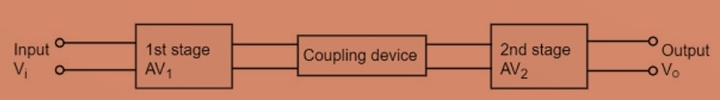
Multistage Amplifier Circuit Diagram
Bipolar Junction Transistor (BJT) is the basic transistor among all the transistors. If we study and understand the working of Multistage amplifiers using BJTs, then it will be easy to understand the working of multi-stage amplifiers using JFET or MOSFET. The simple block diagram of the Multistage amplifier is shown in the figure below.
- Let Av_1, Av_2, Av_,…, Av_n be the voltage gains of ‘n’ single-stage amplifiers connected in cascaded form. Then, the overall voltage gain of the Multistage amplifier will be equal to the product of voltage gains of those ‘n’ single-stage amplifiers. Mathematically, it can be represented as Av= Av_1, Av_2, Av_,…, Av_n.
- Let fc_1& fc_2 be the lower and higher cut-off frequencies of all the ‘n’ single-stage amplifiers connected in cascaded form. Then, the overall lower and higher cut-off frequencies of the Multistage amplifier will be Fc_1& Fc_2, respectively.
- Fc_1=fc_1/ √(21/n-1).
- Fc_2=fc_2 *√(21/n-1).
- The bandwidth of the Multistage amplifier, BW = Fc_2-Fc_1.
Configurations of Multistage Amplifier
We will get the number of stages between the input and output of a multistage amplifier based on the number of transistors in the circuit. For easy understanding, let us consider the amplifiers to have two stages. We have three types of single-stage amplifiers based on the configuration of the transistor. These are Common Base (CB), Common Emitter (CE), and Common Collector (CC) configurations.
The possible two-stage amplifiers are CB-CB, CB-CE, CB-CC, CE-CB, CE-CE, CE-CC, CC-CB, CC-CE, and CC-CC. Based on the requirement, we will use the respective two-stage amplifier. We must couple the AC output of one stage as the AC input for the other stage. Based on the types of coupling between the stages, we will get the following configurations of Multistage amplifiers, which have two stages each.
- Impedance Coupled Amplifier
- Cascode Amplifier
- Transformer Coupled Amplifier
- Direct Coupled Amplifier
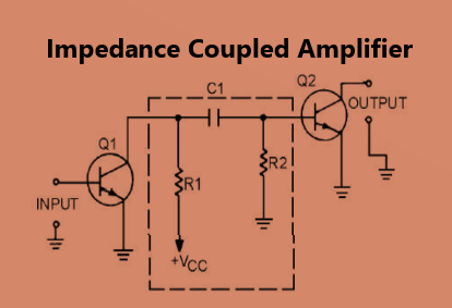
Impedance Coupled Amplifier
If the two transistors (stages) of a Multistage amplifier are coupled through the combination of resistor and capacitor, it is known as impedance coupling or RC coupling. In this configuration, we will connect two CE amplifiers in cascaded form with an impedance coupling. Hence, this amplifier is called an RC coupled amplifier, CE-CE amplifier, or Cascade amplifier. The circuit diagram of this configuration is shown below.
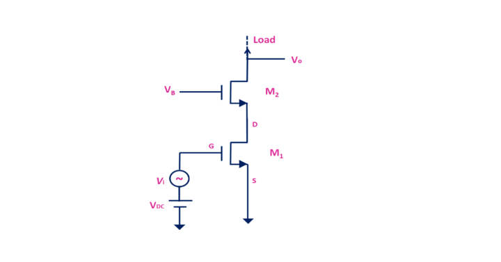
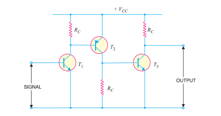
Cascode Amplifier
In the Cascode connection, both the transistors will be in series. In this configuration, we will connect CE and CB amplifiers in such a way that the transistor of the CB amplifier will lie on top of the transistor of the CE amplifier. The advantage of the Cascode connection is that it provides the value of input impedance as high. The circuit diagram of the Cascode connection of the Multistage amplifier, which has two stages, is shown below.
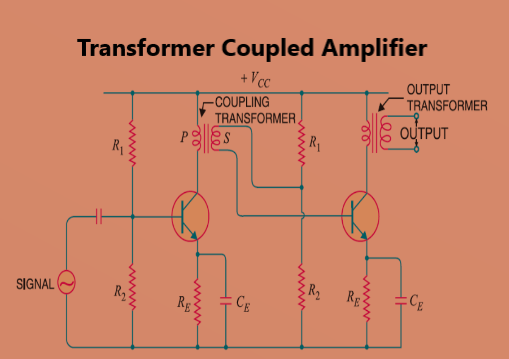
Transformer Coupled Amplifier
If the two transistors (stages) of a Multistage amplifier are coupled through the transformer, it is known as transformer coupling. In this configuration, we will connect two CE amplifiers in cascaded form with a transformer coupling. In general, we will use this configuration at the amplifier system’s last stage since it helps impedance matching. The circuit diagram of this configuration is shown below.
Direct Coupled Amplifier
If the two transistors (stages) of a Multistage amplifier are directly connected, then it is known as Direct coupling. In this configuration, we will connect two CC amplifiers so that the emitter current of one transistor (first stage) will be the base current of another transistor (second stage). This configuration is also known as the Darlington configuration. The current gain of this configuration will be the product of the current gains of both transistors. The circuit diagram of this configuration is shown below.
If you are preparing for GATE and ESE, avail Online Classroom Program to get unlimited access to all the live structured courses and mock tests from the following link: