- Home/
- GATE ELECTRONICS/
- GATE EC/
- Article
PN Junction Diode
By BYJU'S Exam Prep
Updated on: September 25th, 2023

As the name implies, the p-n junction diode consists of two semiconductors types: p-type and n-type. This diode is the basic one among all the diodes. Once you understand the p-n junction forward and reverse bias, it will be easy to understand the biasing of any other diode.
To understand the working of any other diode easily, one must first understand the working of the p-n junction diode. In this article, get an overview of the p-n junction diode. In addition, you will learn about the depletion region and the types of biasing in the p-n junction diode. And then the V-I characteristics of the p-n junction diode.
Table of content
What is p-n Junction Diode?
We have two types of semiconductor materials, namely p-type and n-type. One interface or junction forms when we keep these two sides by the side inside a single semiconductor crystal. That junction is known as the p-n junction.
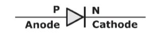
p-n Junction Diode Symbol
As the name of the diode implies, it has two electrodes called cathode and anode. The symbol of the p-n junction diode is shown in the following figure. Here, the triangle symbol indicates the direction of current flow from the p side to the n side.
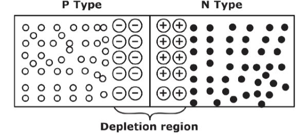
Depletion Region in p-n Junction Diode
We know that in p-type semiconductors, holes are the majority of charge carriers. Whereas in n-type semiconductors, electrons are the majority charge carriers. When we keep a p-type material adjacent to an n-type material, the excess electrons will initially move from the n-region to the p-region and combine with excess holes of this region. After that, the n-region becomes positively charged since it loses the electrons. Whereas the p-region becomes negatively charged since it accepts the electrons.
After some time, the further movement of electrons from n-side to p-side will be stopped because of repelling due to the negative charge of the p-region. Similarly, the further movement of holes from the p-side to the n-side will be stopped because of repelling due to the positive charge of the n-region. Due to this, some regions on both sides of the p-n junction have no mobile charge carriers. Hence, this region is called the Depletion region. It acts as an insulator between the two regions of the p-n junction diode. This region is also called the depletion layer or space charge region.
p-n Junction Diode Biases
Since the immobile ions are present in the depletion layer, it becomes a barrier for electrons to move from the n-side to the p-side and similarly for holes to move from the p-side to the n-side. The minimum potential required for electrons to move from the n-side to the p-side, is known as barrier potential or cut-in voltage.
The cut-in voltages of Germanium (Ge) and Silicon (Si) diodes are 0.3 V and 0.7 V, respectively. For this, we must supply externally to the diode, which is known as bias. Now, let us discuss the following two types of p-n junction diode Biases.
- p-n junction diode in forward bias
- p-n junction diode in reverse bias
p-n Junction Diode in Forward Bias
If the positive and negative terminals of the battery are connected to the p-region and n-region of the p-n junction diode, respectively, then we will say that the p-n junction diode is in forward bias. In short, we can call that bias a p-n junction forward bias. This circuit diagram is shown in the below figure.
The forward biased p-n junction diode act as a short circuit.
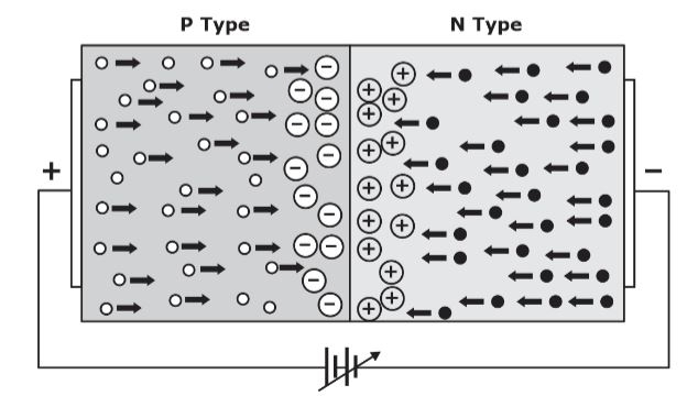
Due to this forward bias, electrons will move from the n-region to the p-region via the p-n junction. Hence, the width of the depletion layer will be reduced. Once again, the electron-hole recombination will take place in the p-region. So, in the forward bias, the current will flow from the p-region to the n-region. In the p-region, the current is due to holes. Whereas in the n-region, the current is due to electrons.
p-n Junction Diode in Reverse Bias
If the negative and positive terminals of the battery are connected to the p-region and n-region of the p-n junction diode, respectively, then we will say that the p-n junction diode is in reverse bias. In short, we can call that bias the p-n junction reverse bias. This circuit diagram is shown in the below figure.
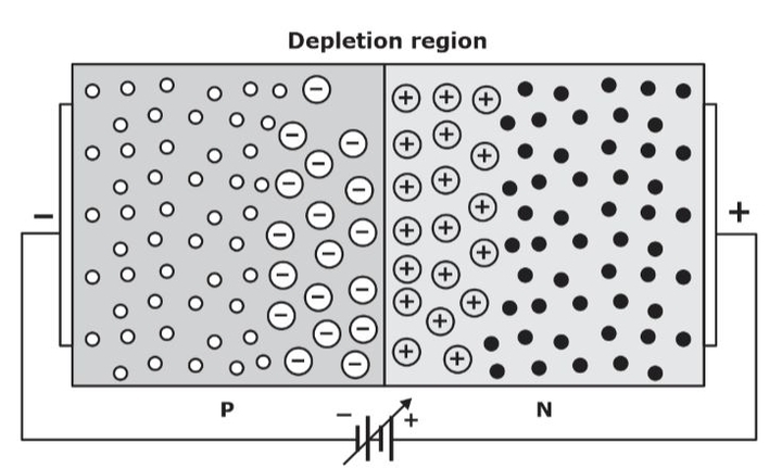
Due to this reverse bias, electrons and holes are attracted back toward the battery. Because of this, the width of the depletion region will increase. So, in the reverse bias, the current will not flow from the p-region to the n-region.
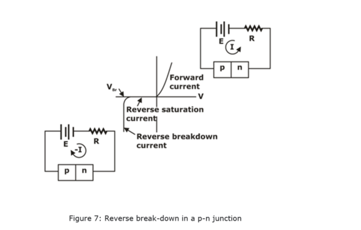
Reverse Bias Breakdown in p-n Junction Diode
We found that a p-n junction biased in the reverse direction exhibits a small, voltage-independent saturation current. This is true until a critical reverse bias is reached, for which reverse breakdown occurs. At this critical voltage (VBr) the reverse current through the diode increases sharply, and relatively large currents can flow with little further increase in voltage.
The reverse biased p-n junction diode act as a an insulator.
The existence of a critical breakdown voltage introduces almost a right-angle appearance to the reverse characteristic of most diodes.
V-I Characteristics of p-n Junction Diode
Since the p-n junction diode allows the flow of negatively charged particles (electrons) only in the Forward bias, it is called a unilateral element.
The barrier voltage of a p-n junction diode depends on:
- semiconductor material,
- doping
- temperature and
- biasing
Hence, we can use p-n junction diodes in rectifiers for converting AC into DC. The V-I characteristics of the p-n junction diode (practical) are shown in the below diagram.
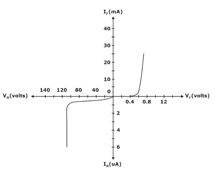
The forward bias current of the p-n junction diode will be in the order of milli-Amperes or Amperes. The reverse bias current of the p-n junction diode will be in the order of micro-Amperes or nano-Amperes.