- Home/
- GATE ELECTRONICS/
- GATE EC/
- Article
Integrated Circuits
By BYJU'S Exam Prep
Updated on: September 25th, 2023

Integrated circuits are ubiquitous around us, and we don’t even realize it. The functionality of the Integrated Circuits within devices like Laptops, smartphones, tablets, desktop computers, refrigerators, televisions, digital clocks, or any other electronics we come across every day. Integrated circuits have wide applications in automobiles as well.
Integrated circuits are generally electronic circuits present in our day-to-day devices. Integrated circuits are responsible for transferring electric current flow to different kinds of components such as diodes, transistors, resistors, capacitors, and inductors. Integrated circuits are microscopic.
Download Formulas for GATE Electronics & Communication Engineering – Control System
Table of content
What is Integrated Circuit?
Integrated circuits compose the major portion of the field of microelectronics and may consist of film, monolithic or hybrid circuits. The integrated circuit comprises active and passive components formed by diffusion into a single silicon chip, with interconnection provided by an aluminum metallization process.
Definition of Integrated Circuit
An integrated circuit is a miniaturized, low-cost electronic circuit consisting of active and passive components fabricated on a substrate. The active components are diodes and transistors, while all passive components are resistors and capacitors.
Download Formulas for GATE Electronics & Communication Engineering – Digital Circuits
Who Invented Integrated Circuit?
The Observation made by Gorden Moore refers to Moore’s Law in 1965 that the number of transistors doubles every two years in a dense integrated circuit. At the same time, Robert Noyce is known to be the inventor of the first monolithic integrated circuit.
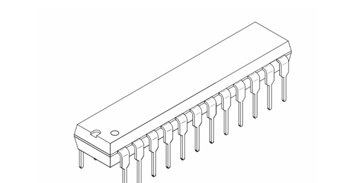
Integrated Circuit Diagram
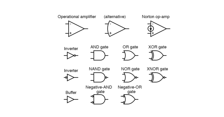
Integrated Circuit Symbol
Here are the symbols of a few Integrated circuits:
Types of Integrated Circuit
Certain logic techniques and circuit designs are used to design an integrated circuit. Three categories of IC design are the following, namely Analog, Digital, and Mixed Design. A detailed description of each Integrated circuit design is mentioned below:
- Analog Design: Analog design in the context of integrated circuit (IC) design is a discipline that focuses on creating circuits that operate in and are optimized for continuous time-domain behavior. Typical objectives of analog design include Signal fidelity, Amplification, and Filtering. When the term integrated circuit design comes across, most people think of the design of complex microprocessors. These circuits are designed using digital design techniques, which focus on the propagation of discrete values, i.e., ones and zeros. It’s important to understand that this propagating ones and zeros model is used to simplify the analysis of huge networks. The actual devices in any circuit respond to continuously varying stimuli, so analog circuit design is the foundation of the design of digital circuits.
- Digital Design: Digital IC design produces components such as microprocessors, FPGAs, memories (RAM, ROM, and flash), and digital ASICs. The digital design focuses on logical correctness, maximizing circuit density, and placing circuits, so that clock and timing signals are routed efficiently.
- Mixed Design: The mixed-signal design integrates digital and analog design principles. The mixed integrated Circuits function as Digital to Analog converters, Analog to Digital converters (DAC and ADC converters), and clock/timing ICs.
Download Formulas for GATE Electronics & Communication Engineering – Electronic Devices
Integrated Circuit Advantages
Over the years, we have observed how technology has squeezed itself into a more compact and concise structure. For instance, the first computers made were the size of 1000 laptops we use today. So how has this been made possible? The answer is Integrated Circuits.
- Miniaturization and hence increased equipment density.
- Batch processing results in cost reduction.
- Improve system reliability due to the elimination of soldered joints.
- Better functional performance.
- Matched Devices.
- Increased operating speed.
- Significant reduction in power consumption.
What are the Importance Classifications of Integrated Circuit?
Based on the number of gates per chip, below are the classification of different types of integrated Circuits based on their chip size. The basic classifications are SSI, MSI, LSI, and VLSI. ULSI is now in the talk, which stands for the Ultra-large scale of Integration.
- Small Scale Integration (SSI) : 3 to 30 gates/chip.
- Medium Scale Integration (MSI) : 130 to 300 gates/chip.
- Large Scale Integration (LSI) : 300 to 3000 gates/chip.
- Very Large Scale Integration (VLSI) : 3 to 30 gates/chip.
What are Monolithic Integrated Circuits and Their Limitations?
The word ‘monolithic’ comes from the Greek word ‘Monos’ and ‘Lithos’, which means ‘single’ and ‘Stone’. So the monolithic integrated circuits refer to a single stone or a single crystal. The single crystal means a single silicon chip as a semiconductor material, on top of which all the passive and active components are connected.
Monolithic ICs are considered the best mode of manufacturing Integrated Circuits as :
- It can be made identical.
- High Reliability.
- Manufactured in bulk in a brief period.
- Low cost.
Limitations of Monolithic Integrated Circuit:
- Low power Ratings
- It can be used for high-power applications as it can not have more power rating than 1W.
- The isolation between components within the integrated circuit is poor.
- Components such as inductors can not be fabricated.
- The passive components within the Integrated circuit will have a small value, and an external connection is required from the Integrated circuit pins to obtain high values.
- Flexible circuits are not possible.
Fabrication of Integrated Circuit
The monolithic fabrication consists of various processes such as wafer preparation, circuit probing, base and emitter diffusions, pre-ohmic etch, metallization, epitaxial growth, diffused isolation, wire bonding, encapsulation, dicing, mounting and packaging, and final testing.
- Each diffusion process involves a silicon dioxide layer, photoresist mask, ultraviolet exposure, etching, scrubbing, and diffusion.
- Practical IC resistance values range from 25 Ω to 500 k Ω, depending upon the sheet resistivities measured in ohms per square. For example, P-type diffused resistors have values from 50 to 250 Ω per square, and pinch resistors have a value of 5000 Q per square.
- Because the tolerances of resistance values are at best ±30%, ICs are designed to utilize resistance ratios, which may be controlled to within 3%.
- Capacitors may be obtained using the p-n junctions in transistor-type structures or the MOS capacitive effects employing the silicon-dioxide layer. Practical values range from 3 to 30 pF because of the excessive area used for larger values.
- By suitable interconnecting COS/MOS ICs, an inverter circuit with very low quiescent dissipation can be made available. Furthermore, many of the logic gates in digital systems may be implemented by further interconnecting many inverters.
- Integrated circuits may be of the monolithic or hybrid type, with the latter being a mixture of thin-film and diffused components.
- Complementary Symmetry MOS ICs (COS/MOS) involve a p-channel and an n-channel MOSFET fabricated on the same chip.
- Large Scale Integration (LSI) involves the fabrication of 100 or more logic gates on a single chip, while Medium Scale Integration (MSI) is defined as more than 12 but less than 100 gates on a single chip.
Fabrication Process
The fabrication of integrated circuits consists basically of the following process steps:
- Lithography: The process for pattern definition by applying a thin uniform layer of viscous liquid (photoresist) on the wafer surface. The photoresist is hardened by baking and selectively removed by light projection through a reticle containing mask information.
- Etching: Selectively removing unwanted material from the surface of the wafer. The pattern of the photoresist is transferred to the wafer using etching agents.
- Deposition: Films of various materials are applied to the wafer. For this purpose, two processes are mostly used: physical vapor deposition (PVD) and chemical vapor deposition (CVD).
- Chemical Mechanical Polishing: A planarization technique applying chemical slurry with etchant agents to the wafer surface.
- Oxidation: In the oxidation process, oxygen (dry oxidation) or H2O (wet oxidation) molecules convert silicon layers on top of the wafer to silicon dioxide.
- Ion Implantation: Most widely used technique to introduce dopant impurities into the semiconductor. The ionized particles are accelerated through an electrical field and targeted at the semiconductor wafer.
- Diffusion: A diffusion step following ion implantation is used for annealing bombardment-induced lattice defects.
Oxidation
- It is a process that converts silicon on the wafer into silicon dioxide.
- The chemical reaction of silicon and oxygen already starts at room temperature but stops after a very thin native oxide film.
- The wafer must be settled in a furnace with oxygen or water vapor at elevated temperatures for an effective oxidation rate.
- Silicon dioxide layers are used as high-quality insulators or masks for ion implantation.
- Silicon can form high-quality silicon dioxide.
Diffusion
- Diffusion is the movement of impurity atoms in a semiconductor material at high temperatures.
- The driving force of diffusion is the concentration gradient.
- There is a wide range of diffusivities for the various dopant species, which depend on how easily the respective dopant impurity can move through the material.
- Diffusion is applied to anneal the crystal defects after ion implantation or to introduce dopant atoms into silicon from a chemical vapor source.
- In the last case, the diffusion time and temperature determine the depth of dopant penetration.
- Diffusion forms the source, drain, and channel regions in a MOS transistor.
- But diffusion can also be an unwanted parasitic effect because it occurs during all high-temperature process steps.
Ion Implantation
- Ion Implantation is the process of adding impurities to a silicon wafer.
- This is performed with an electric field that accelerates the ionized atoms or molecules so that these particles penetrate the target material until they come to rest because of interactions with the silicon atoms.
- Ion implantation can control exactly the distribution and dose of the dopants in silicon because the penetration depth depends on the kinetic energy of the ions, which is proportional to the electric field. Therefore, the dopant dose can be controlled by varying the ion source.
- Unfortunately, the crystal structure is damaged after ion implantation, which implies worse electrical properties.
- Another problem is that the implanted dopants are electrically inactive because they are situated on interstitial sites.
- Therefore, a thermal process step is necessary after ion implantation, which repairs the crystal damage and activates the dopants.
Photolithography
- Lithography is used to transfer a pattern from a photomask to the surface of the wafer.
- Photolithography is the process of creating patterns on a smooth surface (Silicon wafer).
- This is accomplished by selectively exposing parts of the wafer while other parts are protected. The exposed sections are susceptible to doping, removal, or metallization. Specific patterns can be created to form conductors, insulators, or doping regions. Putting these patterns onto a wafer is called photolithography.
- The pattern defined by the mask is either removed or remained after development, depending if the type of resistance, is positive or negative.
Etching
- Etching is used to remove material selectively to create patterns.
- The etching mask defines the pattern because the parts of the material, which should remain, are protected by the mask.
- The unmasked material can be removed by wet (chemical) or dry (physical) etching.
Twin-tub CMOS Process
- It is also possible to create both a p-well and an n-well for the n-MOSFETs and p-MOSFET, respectively, in the twin well or twin tub technology. Such a choice means that the process is independent of the dopant type of the starting substrate (provided it is only lightly doped).
- Provide separate optimization of the n-type and p-type transistors.
- The threshold voltage, body effect, and channel transconductance of both transistors can be tuned independently.
- Generally, the starting material is a p+ or n+ substrate, with a lightly doped epitaxial layer on top. This epitaxial layer provides the actual substrate on which the n-well and the p-well are formed.
- Since two independent doping steps are performed to create good regions, the dopant concentrations can be carefully optimized to produce the desired device characteristics.