- Home/
- GATE ELECTRONICS/
- GATE EC/
- Article
Bipolar Junction Transistor
By BYJU'S Exam Prep
Updated on: September 25th, 2023

A BJT is a three-terminal semiconductor device that consists of two p-n junctions, which are used to amplify or magnify a signal. The full form of BJT is a bipolar junction transistor. It is a currently controlled device. The terminals of the BJT are the emitter, collector, and base. BJT is bipolar because it uses electrons and holes as charge carriers. There are two types of bipolar junction transistors: NPN and PNP.
In this article, you’ll get to know about the working principle of BJT, its equivalent circuit, various configurations, which are common base (CB), common emitter (CE), and common collector (CC), its input and output characteristics, and various applications.
Table of content
What is BJT?
BJT stands for Bipolar Junction Transistor, is a current-controlled semiconductor device that controls the amount of current flowing through it. A small current flowing into the base terminal controls the collector current.
Types of Bipolar Junction Transistor
There are the following two types of BJT
- PNP BJT
- NPN BJT
The diagram below shows that BJT has three parts: emitter, base, and collector. There are two junctions which are the emitter junction and the collector junction.
BJT Diagram
![]()
Suppose we join together two individual signal diodes back-to-back. In that case, this will give us two PN-junctions together in series which would share a common Positive, (P) or Negative, (N) terminal. The fusion of these two diodes produces a three-layer, two junctions and a three-terminal device ,is formed which is the basis of a Bipolar Junction Transistor.
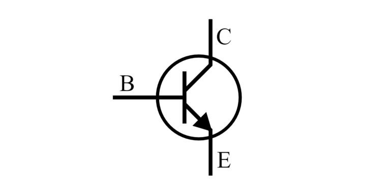
BJT Symbol
The figure given below shows the symbol of BJT:
BJT Circuit Diagram
Working Principle of BJT
For the n-p-n transistor biased to be in the active region, the BE(base-emitter) junction is forward biased whereas the CB(collector-base) junction is reverse biased. The width of the basecorner junction’s depletion region is small compared to that of the CB junction. The forward bias at the base-emitter junction reduces the barrier, potential and due to this, the electrons flow from the emitter to the base. The base is thin and lightly doped as it contains very few holes so some of the electrons from the emitter recombine with the holes in the base region and flow out of the base terminal. This constitutes the base current, it flows due to the recombination of electrons and holes. The ring huge number of electrons will cross the collector junction(reverse biased) to constitute the collector current. Thus by KCL,
IE = IB + IC
The base cutinyery small as compared to the emitter and collector current. Therefore, IE = IC
In NPN BJT, the majority of charge carriers are electrons. The operation of a PNP transistor is the same as that of an NPN transistor; the only basic difference is that most charge carriers are holes instead of electrons. BJT is called minority carrier devices because only a small part of current flows is due to majority carriers, and most current flows are due to minority charge carriers.
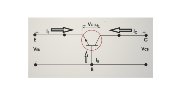
BJT Biasing
A BJT has two pn-junctions which are the emitter-base junction and collector-base junction. The application of DC voltages at the two junctions of the BJT is known as Biasing.
- Transistor as an amplifier– The emitter-base junction is forward-biased, and the collector-base junction is reverse-biased. Transistor operated under this bias condition is said to operate in the active region.
- Transistor as a switch- When both junctions are forward-biased, the transistor operates in the saturation region. The transistor operated in the saturation region acts like a closed switch, and the collector current is maximum.
- Transistor as an open switch- When both the junctions are reverse-biased, the transistor operates in the cut-off region. The BJT operating in the cut-off region acts as an open switch, and a very small collector current flows from emitter to collector. This is called reverse leakage current due to minority charge carriers.
BJT Configurations
There are three possible ways to connect a Bipolar junction transistor with an electronic circuit, with one terminal common to both the input and output signals.
- Common Base – The base connection is common to both the input and the output signal. The input signal is applied between the transistors’ base and the emitter terminals, while the output signal is taken from between the base and the collector terminals. The base terminal is grounded. The input current flowing into the emitter is the sum of both the base and collector current; the collector current is less than the emitter current resulting in a current gain for this type of circuit of unity or less.
- Common Emitter – The input signal is applied between the base and the emitter, while the output is taken from between the collector and the emitter. The common emitter amplifier configuration produces the highest current and power gain of all three bipolar transistor configurations. It is mainly because the input impedance is low while the output impedance is high.
- Common Collector – The collector is connected to the ground, and the collector terminal is common to both the input and the output. The input signal is connected directly to the base terminal, while the output signal is taken from the emitter load. This configuration is commonly known as a Voltage Follower or Emitter Follower circuit. It is useful for impedance matching applications because of its very high input impedance and relatively low output impedance.
BJT Characteristics
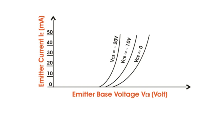
Input characteristics of a Common Base configuration are shown below. The input current is the emitter current, and the input voltage is the emitter-base voltage. Emitter current increases for fixed emitter-base voltage when collector-base voltage increases.
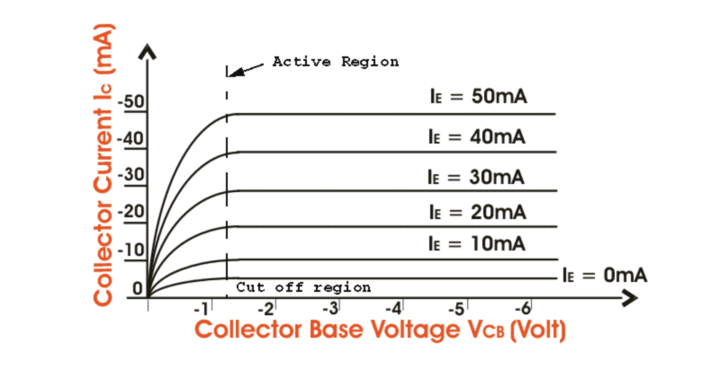
The output characteristics show the relation between the output voltage and output current. The Collector current is the output current and collector-base voltage, and the emitter current is the input current and works as the parameters. The figure below shows the output characteristics for a p-n-p transistor in CB mode. Similarly, the common-emitter and Common collector configurations have input and output characteristics, respectively.
Applications of BJT
Bipolar junction transistors have a low forward voltage. They can be operated in low to high-power applications. They have a large gain bandwidth. BJT has greater gain than FET. They are cheaper to manufacture. The switching time of BJT is medium in comparison to FET. They are applicable for low-current applications. They have a negative temperature coefficient. Below are some applications of BJT.
- The BJT is used as an oscillator, amplifier, and multivibrator.
- It is used in clipping circuits for wave shaping.
- Used in timer and delay circuits.
- Used as electronic switch, detector, and demodulator.
- Used in switching circuits.