- Home/
- GATE ELECTRONICS/
- GATE EC/
- Article
Fermi Level – Definition, Application, Intrinsic and Extrinsic
By BYJU'S Exam Prep
Updated on: September 25th, 2023

The Fermi Level is the maximum energy level that an electron may occupy when it is at absolute zero degrees Fahrenheit. Since the electrons are all in the lowest energy state at absolute zero, the Fermi level is located between the valence band and conduction band. Semiconductor materials play a vital role in the field of electronics. In electronic devices like diodes & transistors (BJT, JFET, MOSFET) and even in IC technology, we are using semiconductor materials. The position of the Fermi Level determines the type of semiconductor material. It changes (moves) when there is temperature variation and/or by adding impurities to the semiconductor. So, based on the requirement and application we must keep the position of the Fermi level in the semiconductor appropriately.
From this article, you will get an overview of the semiconductor Fermi level. First, you will get to know the definition of this energy level and the Fermi-Dirac distribution function and then the Fermi Level formula, along with the Fermi level in semiconductors like intrinsic and extrinsic (n-type & p-type).
Download Formulas for GATE Electronics & Communication Engineering – Control System
Table of content
What is Fermi Level?
The Set (group) of energy levels is known as the energy band. In the energy band diagram, there are mainly two energy bands. Those are the conduction band and valence band. The region between these two energy bands is known as the forbidden energy gap or energy gap in short.
Fermi level is an energy level, which lies in the energy band diagram. It distinguishes the set of levels that are occupied with electrons from the set of levels that are not occupied with electrons. We can define the Fermi level in two ways.
- It is the minimum energy level, beyond which all the levels are not occupied with electrons (empty) at T=0K.
- It is the maximum energy level, below which all the levels are filled with electrons at T=0K.
Download Formulas for GATE Electronics & Communication Engineering – Digital Circuits
What is Fermi-Dirac Distribution Function?
By using the Fermi-Dirac distribution function, we will get to know the probability of occupancy of energy levels by negatively charged particles (electrons).
Fermi Level Formula
Let, E be the energy level at which the electrons are occupied, and T be the absolute temperature. Mathematically, the Fermi-Dirac distribution function is represented as
f(E)=1/(1+e(E-EF/ kT))
Where,
- EF is the Fermi energy level or Fermi level in short and k is Boltzmann’s constant.
- k=1.38×10⁻²³ J/K=8.62×10-5 eV/K.
- f(E)=1 for E
- f(E)=0 for E>EF and at T=0 K.
- f(E)=0.5 for E=EF and at T>0 K.
- f(E)= 1/e(E-EF/ kT)=e-(E-EF/ kT) for E-EF≫kT
Fermi Level in Semiconductor
The energy band gap is nothing but the difference between the lowest level of the conduction band and the highest level of the valence band. A material is said to be a semiconductor if its energy bandgap is greater than that of a conductor and less than that of an insulator.
That means the energy bandgap of the semiconductor lies between that of the conductor and insulator. Fermi level for extrinsic semiconductors depends on the number of impurities that are added to the intrinsic semiconductor. Since we are having two types of semiconductors, now let us discuss the energy level in those two types one by one.
- Fermi Level in Intrinsic Semiconductor
- Fermi Level in Extrinsic Semiconductor
Download Formulas for GATE Electronics & Communication Engineering – Electronic Devices
Fermi Level in Intrinsic Semiconductor
Intrinsic semiconductors are also called undoped semiconductors since there are no impurities. In an intrinsic semiconductor, the number of electrons and holes are the same.
Fermi Level in Intrinsic Semiconductor Formula
The relation of the Fermi-Dirac distribution function between the conduction band and valence band in an intrinsic semiconductor can be represented as
f(EC)=1-f(EV)
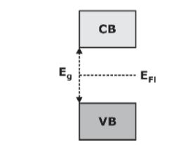
=> EF=(EC+EV)/2=EFi
Where EFi is the Fermi level in an intrinsic semiconductor. In an intrinsic semiconductor, EFi lies exactly in the middle of the energy gap. That means, it lies exactly in between the conduction and valence bands. The following diagram illustrates this one.
Fermi Level in Extrinsic Semiconductors
If we add the impurities to the intrinsic semiconductor for improving the conductivity, then that material is called an extrinsic semiconductor. The process of adding impurities to the intrinsic semiconductor is known as doping. Due to doping, the number of electrons and holes will differ in this material.
Electrons are called negative charge carriers whereas holes are called positive charge carriers. The absence of electrons is nothing but holes. The Fermi level for extrinsic semiconductors depends on
- the temperature,
- impurity concentration, and
- donor element
Since we are having two types of extrinsic semiconductors, now let us discuss the Fermi level in those two types one by one.
Fermi Level in n-type Semiconductor
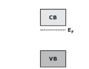
Electrons are the majority charge carriers in the n-type semiconductor. In an n-type semiconductor, the value of EC-EF is positive and it is equal to kT ln(NC/ND). That means, the Fermi level lies below the conduction band, and it is closer to the conduction band. The diagram of the Fermi level in n-type semiconductors is shown in the figure below.
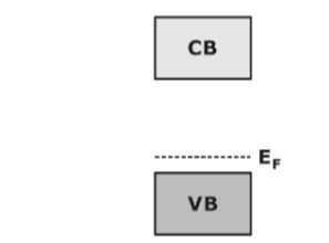
Fermi Level in p-type Semiconductors
Holes are the majority charge carriers in the p-type semiconductor. In p-type semiconductors, the value of EF-EV is positive and it is equal to kT ln (NV/NA). That means, the Fermi level lies above the valence band, and it is closer to the valence band. The diagram of the Fermi level in p-type semiconductors is shown in the figure below.