- Home/
- GATE ELECTRONICS/
- GATE EC/
- Article
Logic Families Study Notes for GATE EC
By BYJU'S Exam Prep
Updated on: September 25th, 2023

Logic Families Study Notes for GATE EC are a valuable resource designed to help you master the intricate concepts of logic families. This study notes offer a comprehensive overview of various logic families, their characteristics, and their applications in the context of the GATE EC exam. By delving into the depths of Logic Families Study Notes for GATE EC, you will gain a solid foundation in understanding the functioning and behaviour of different logic families. With Logic Families Study Notes for GATE EC, you can enhance your understanding of the subject and develop a strong grasp of the underlying principles. These study notes provide a systematic approach to learning about logic families, allowing you to explore topics such as TTL, CMOS, ECL, and more.
By repetitively emphasizing the importance of Logic Families Study Notes for GATE EC, this resource ensures that you gain the necessary knowledge and confidence to excel in the exam. Logic Families Study Notes for GATE EC cover a wide range of topics, including the advantages and disadvantages of different logic families, their power consumption, noise immunity, propagation delay, and fan-out capabilities. By studying these notes, you will learn how to choose the most appropriate logic family for a given application, taking into consideration factors such as speed, power requirements, and environmental conditions. Whether you are a beginner or an experienced GATE EC aspirant, these study notes will provide you with the insights and expertise needed to tackle logic family-related questions with ease.
Check out: Top Ten Preparation Tips for GATE Exam
Table of content
-
1.
Introduction to Logic Families

-
2.
Understanding the Characteristics of Different Logic Families in GATE EC
-
3.
Applications of Logic Families
-
4.
Choosing the Right Logic Family
-
5.
Integrated Circuits
-
6.
Characteristics of digital circuits
-
7.
Digital IC Terminology
-
8.
Diode Logic (DL)
-
9.
Resistor-Transistor Logic (RTL)
-
10.
Diode-Transistor Logic (DTL)
-
11.
Transistor-transistor logic (TTL)
-
12.
Types of TTL
Introduction to Logic Families
Logic families form the fundamental building blocks of digital electronic circuits, playing a crucial role in the field of electronics and communication engineering. In the context of GATE EC (Electronics and Communication Engineering) exam preparation, a solid understanding of logic families is essential. An introduction to logic families provides aspiring candidates with a comprehensive overview of the different types of logic families, their characteristics, and their applications in various electronic devices. Logic families can be broadly classified into categories such as TTL (Transistor-Transistor Logic), CMOS (Complementary Metal-Oxide-Semiconductor), ECL (Emitter-Coupled Logic), and more. Each logic family has its unique characteristics, advantages, and limitations, making it crucial for GATE EC aspirants to grasp their functioning.
Logic families are sets of chips that may implement different logical functions but use the same type of transistors and voltage levels for logical levels and for power supplies. These families vary by speed, power consumption, cost, and voltage-current levels. The most widely used families are:
- DL (Diode- logic)
- DTL (Diode-transistor logic)
- RTL (Resistor-transistor logic)
- TTL (Transistor -transistor logic)
- ECL (Emitter-coupled logic)
- MOS (Metal-oxide semiconductor)
- CMOS (Complementary Metal-oxide semiconductor)
Understanding the Characteristics of Different Logic Families in GATE EC
When studying for the GATE EC exam, it is essential to grasp the characteristics of different logic families thoroughly. Logic families refer to a set of electronic circuits with specific characteristics, operating voltages, noise margins, and power consumption. Each logic family has its unique advantages and disadvantages, making it crucial for GATE EC aspirants to understand their intricacies.
One commonly encountered logic family is the Transistor-Transistor Logic (TTL), which is known for its compatibility with both bipolar and CMOS technologies. TTL logic families offer fast switching speeds and robust noise immunity, making them suitable for high-performance applications. However, they tend to consume more power compared to other families and have limited fan-out capabilities.
Applications of Logic Families
Logic families find diverse applications in various fields, and understanding their practical uses is crucial for GATE EC aspirants. One prominent application of logic families is in digital integrated circuits (ICs). These ICs serve as the building blocks of modern electronic devices, ranging from smartphones and computers to industrial control systems. Different logic families, such as TTL (Transistor-Transistor Logic), CMOS (Complementary Metal-Oxide-Semiconductor), and ECL (Emitter-Coupled Logic), are utilized based on specific requirements.
TTL logic families, known for their robustness and high-speed operation, are commonly employed in applications where fast switching times and noise immunity are crucial. They find extensive use in microprocessors, memory chips, and data communication systems. On the other hand, CMOS logic families are highly power-efficient, making them ideal for portable devices with limited battery life. They are widely employed in devices such as smartphones, tablets, and wearable technology. Furthermore, ECL logic families, characterized by their high-speed operation and low power consumption, are often used in high-frequency applications like telecommunications and radar systems.
Choosing the Right Logic Family
Choosing the right logic family is crucial for achieving success in the GATE EC exam. With various logic families available, each with its unique characteristics and applications, it becomes essential to understand the factors that influence the selection process. When selecting a logic family, one must consider parameters such as speed, power consumption, noise immunity, propagation delay, and fan-out capabilities.
Speed is a vital aspect to consider when choosing a logic family. Different logic families have varying propagation delays, which determine how quickly the output responds to changes in the input. In applications that require high-speed operations, such as high-frequency signal processing or data communication, logic families like ECL (Emitter-Coupled Logic) are often preferred due to their fast switching speeds.
Integrated Circuits
Integrated Circuits (ICs) revolutionized the field of electronics by miniaturizing complex electronic circuits into a single chip. This introductory paragraph highlights the significance of ICs and their transformative impact on various industries.
- Integrated circuits (ICs) are chips, and pieces of semiconductor material, that contain all of the transistors, resistors, and capacitors necessary to create a digital circuit or system.
- The first ICs were fabricated using Ge BJTs in 1958.
- Jack Kirby of Texas Instruments, Nobel Prize in 2000
- Robert Noyes of Fairchild Semiconductor fabricated the first Si ICs in 1959.
Integration Levels:
- SSI Small scale integration [12 gates/chip]
- MSI Medium-scale integration [100 gates/chip]
- LSI Large scale integration [1K gates/chip]
- VLSI Very-large-scale integration [10K gates/chip]
- ULSI Ultra large-scale integration [100K gates/chip]
Moore’s Law:
- A prediction made by Moore (a co-founder of Intel) in 1965: “… a number of transistors to double every 2 years.”
Characteristics of digital circuits
Characteristics of digital circuits refer to the fundamental properties and behaviours exhibited by these circuits, such as binary representation, discrete signal levels, logic operations, and the ability to store and process digital information accurately and reliably.
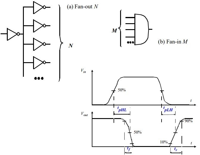
- Fan in:
- Fan-in is the number of inputs connected to the gate without any degradation in the voltage level.
- Fan out:
- Fan out specifies the number of standard loads that the output of the gate can drive without impairment of its normal operation
- Power dissipation:
- Power dissipation is a measure of power consumed by the gate when fully driven by all its inputs.
- Propagation delay:
- Propagation delay is the average transition delay time for the signal to propagate from input to output when the signals change in value. It is expressed in ns.
- Noise margin:
- It is the maximum noise voltage added to an input signal of a digital circuit that does not cause an undesirable change in the circuit output. It is expressed in volts.
Digital IC Terminology
Understanding Digital IC Terminology is essential for anyone working with digital integrated circuits. This introductory knowledge of terms such as logic gates, flip-flops, decoders, and multiplexers provides a foundation for designing and analyzing digital circuits.
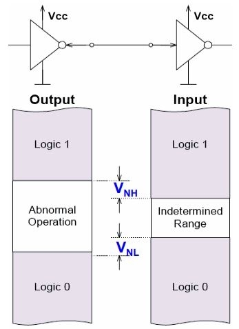
Voltage Parameters:
- VIH(min): high-level input voltage, the minimum voltage level required for a logic 1 at an input.
- VIL(max): low-level input voltage
- VOH(min): high-level output voltage
- VOL(max): low-level output voltage
- For proper operation, the input voltage levels to logic must be kept outside the indeterminate range. Lower than VIL(max) and higher than VIH(min).
Noise Margin:
- The maximum noise voltage that can be tolerated by a circuit is termed its noise immunity (noise Margin)
Current Parameters:
- IOH – Current flowing into output in the logical “1” state under specified load conditions
- IOL – Current flowing into output in the logical “0” state under specified load conditions
- IIH – Current flowing into an input when a specified HI level is applied to that
input - IIL – Current flowing into an input when a specified LO level is applied to that
input
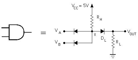
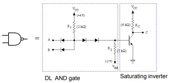
Diode Logic (DL)
Diode Logic (DL) is a simple and fundamental digital logic family that utilizes diodes and resistors to perform logical operations. It provides a basic building block for designing logic circuits and is widely used in various electronic applications.
- simplest; does not scale
- NOT not possible (need an active element)
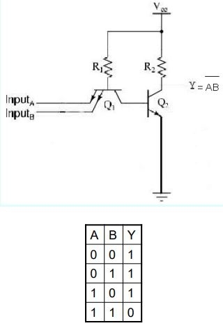
Resistor-Transistor Logic (RTL)
Resistor-Transistor Logic (RTL) is a fundamental digital logic family that uses resistors and transistors to implement logic functions. Explore the basics and applications of RTL in this introductory overview.
- replace the diode switch with a transistor switch
- can be cascaded
- large power draw
Diode-Transistor Logic (DTL)
Diode-Transistor Logic (DTL) is a digital logic family that combines diodes and transistors to perform logical operations. It provides a simple and cost-effective solution for implementing logic circuits with low power consumption and high noise immunity.
- essentially diode logic with transistor amplification
- reduced power consumption
- faster than RTL
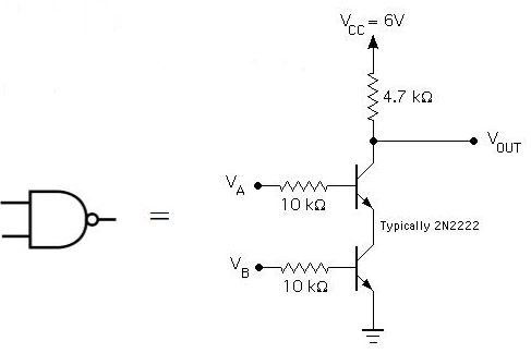
Transistor-transistor logic (TTL)
Transistor-transistor logic (TTL) is a popular digital logic family used in electronic circuits. Known for its simplicity and reliability, TTL utilizes bipolar junction transistors to implement logic gates and functions, making it widely used in various applications.
- based on bipolar transistors one of the most widely used families of small- and medium-scale devices – rarely used for VLSI
- typically operated from a 5V supply
- typical noise immunity about 1 – 1.6 V
- many forms, some optimised for speed, power, etc.
- High-speed versions comparable to CMOS (~ 1.5 ns)
- low-power versions down to about 1 mW/gate
TTL NAND Gate:
- Input terminals: The emitter of Q1
- Output terminals: collector of Q2
- When any input = logic ‘0
- Q1 emitter junction is forward-biased.
- Also, its collector junction is FB,
- so Q1 goes into saturation.
- The base of Q2 is at a Low voltage
- This causes the base-emitter junction of Q2 to be RB, so Q2 goes in cut-off
- Hence the output is 5V or logic ‘1
- When all inputs = logic ‘1
- Q1 emitter junction is RB.
- so Q1 goes in the cut-off.
- Its collector voltage increases
- This forward biases Q2,
- so Q2 goes into saturation
- Hence the output is 0V
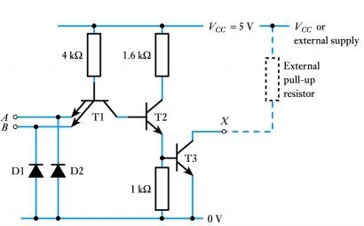
A TTL NAND gate with open collector output:
- It’s similar to the previous circuit.
- Q2 is used as an emitter follower. The output of Q2 is fed to the input of Q3. Collectors of Q2 and Q3 are in phase.
- This circuit needs an external ‘Pull- up resistor between the output and power supply.
- The disadvantage of open- collector gate is their slow switching speed.
- The pull-up resistance is a few kiloohms. Gives a relatively long time constant, when multiplied by the stray output capacitance.
- Is worst when output goes from low to high.
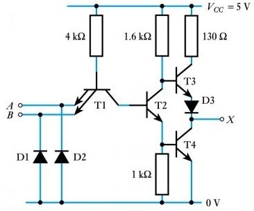
TTL NAND gate with totem pole (active pull-up):
- In this circuit, Q1 and the 4KΩ resistor act like a 2-input AND gate. The remaining circuit acts like an inverter. Transistors Q3 Q4 form a totem-pole i.e.one NPN transistor in series with another.
- With a totem-pole output stage, either Q3 or Q4 is on. When Q3 is ‘on output is high. When Q4 is ‘on output is low. If A or B is low, the Q1 conducts and the base voltage of Q2 is almost zero.
- Q2 cuts off, hence Q4 goes into cut off. Q3 base is high, Q3 acts as an emitter follower, and the output Y is high.
- If A and B are high, Q1 does not conduct (cut-off), and Q2 base goes high (saturation). Q4 goes into saturation hence output is low.
- The drop across Diode D3 keeps the base-emitter diode of Q3 reverse-biased. Hence Q3 is off or else it conducts slightly when output is low.
- Now only Q4 conducts when output is low. Totem pole transistors produce a low output impedance. When Q3 is conducting the output impedance is approx 70 Ω. When Q4 is saturated the output impedance is only 12 Ω. Hence the output impedance of a totem pole circuit is low.
- Any stray output capacitance is rapidly charged or discharged through the low output impedance. Hence the output can change quickly from one state to the other.
Types of TTL
Transistor-Transistor Logic (TTL) is a widely used digital logic family that offers various types of TTL circuits, including standard TTL, Schottky TTL, and Low-Power TTL. Each type has distinct characteristics and applications in electronic systems.
- Standard TTL
- typical gate propagation delay of 10ns and power dissipation of 10 mW per gate, for a power–delay product (PDP) or switching energy of about 100 pJ
- Low-power TTL (L)
- slow switching speed (33ns)
- reduction in power consumption (1 mW) (now essentially replaced by CMOS logic)
- High-speed TTL (H)
- faster switching than standard TTL (6ns)
- but significantly higher power dissipation (22 mW)
- Schottky TTL (S)
- used Schottky diode clamps at gate inputs to prevent charge storage and improve switching time. A Schottky diode has a very low forward voltage drop of 0.15–0.45V approx (silicon diode has a voltage drop of 0.6–1.7V). This lower voltage drop can provide a higher switching speed.
- Faster speed of (3ns) but had higher power dissipation (19 mW)
- Low-power Schottky TTL (LS)
- used the higher resistance values of low-power TTL and the Schottky diodes to provide a good combination of speed (9.5ns) and reduced power consumption (2 mW), and PDP of about 20 PJ.
Get complete information about the GATE exam pattern, cut-off, and all those related things on the BYJU’S Exam Prep official youtube channel.