- Home/
- GATE ELECTRONICS/
- GATE EC/
- Article
Logic Families-2 Study Notes for Electronics and Communication Engineering
By BYJU'S Exam Prep
Updated on: September 25th, 2023

In this article, you will find the Study Notes on Logic Families which will cover the topics such as ECL, MOS Inverter, NAND and NOR with nMOS, CMOS, NAND and NOR with CMOS, Logic Families Comparison.
In this article, you will find the Study Notes on Logic Families which will cover the topics such as ECL, MOS Inverter, NAND and NOR with nMOS, CMOS, NAND and NOR with CMOS, Logic Families Comparison.
1. Emitter-coupled logic (ECL)
- based on bipolar transistors, but removes problems of storage time by preventing the transistors from saturating
- very fast operation – propagation delays of 1ns or less
- high power consumption, perhaps 60 mW/gate
- low noise immunity of about 0.2-0.25 V
- used in some high-speed specialist applications, but now largely replaced by high-speed CMOS
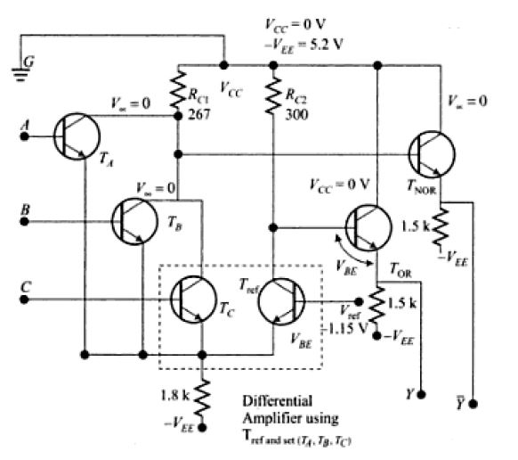
Input:
- Input is at the base of the transistor. The emitter of Tref and input transistors couples together. [Hence the name]
- ECL basic gate is OR/NOR gate
- If any input is not connected, the transistor Ti base-emitter will be at cutoff. Therefore, it will be taken as low logic level
Output:
- The outputs (TOR and TNOR) are taken from the emitters of each transistor. The collector of TOR and TNOR connects to GND in the CC amplifier mode (also called emitter-follower mode).
- The emitter gives the output, which also connects to -VEE through a resistance R (~1.5kΩ)
Differential Amplifier:
- There is transistor T, which forms a differential amplifier pair between T and the parallel circuits of TA, TB, TC. T gets the input reference voltage (VR = -1.15V) from a reference supply circuit.
- The pairs amplify the difference of base voltage of TA (or TB or TC) and Vref.
- The emitters of the differential amplifier pairs connect through a common resistance RE (~1.8kΩ) and to the –VEE(~ -5V)
Emitter Follower (CC) amplifier:
- The collectors of (TA, TB, … ) are also common.
- Common- collectors of the differential amplifier pairs connect through a resistance RC (~267Ω) to the GND
Working:
- Consider TC and Tref
- Case 1: let all Vin = -1.6V. But Vref = -1.15V, so Vin is low and Vref logic high, So TC is in cutoff and Tref in normal inverting mode.
- So TOR gets -1.15V, i.e logic LOW, it is cut off and Y=-VEE (LOW)
- Case 2: If Vin at TC is -0.7V (HIGH), Vref = -1.15V (LOW).
- TC is in normal inverting mode and Tref is in the cutoff. –VEE is reflected at TNOR.
- So TNOR is cut-off. Y’ = -VEE (i.e logic Low).
- TOR is ON, so Y=0v (LOW)
ECL features:
- Faster speed (2 ns propagation delay) of operation than TTL (10 ns), 74S TTL(3 ns)
- More power dissipation (50 mW/gate) than TTL (10 mW), 74S (19mW)
- Noise Margin at ‘1’or ‘0’output and input = 0.4V (– 1.7V and – 1.4V)
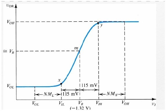
Transfer Characteristics of OR:
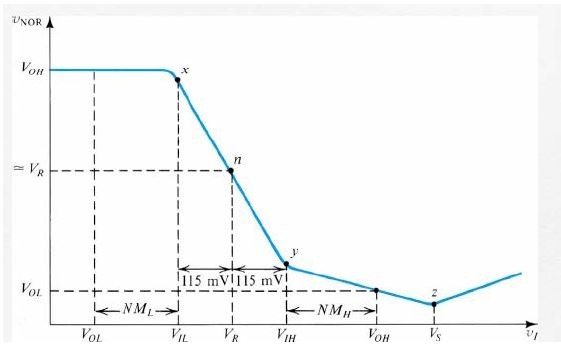
Transfer Characteristics of NOR:
2. MOS inverter
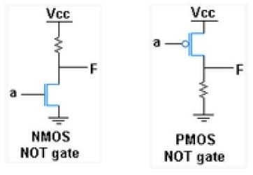
- nMOS Inverter:
- when a=‘1’, nMOS conducts, so F=‘0’
- When a=‘0’, nMOS is cut-off, so F=Vcc=logic ‘1’
- pMOS Inverter:
- when a=‘1’, pMOS is cut-off, so F=‘0’
- When a=‘0’, pMOS is on, so F=Vcc=logic ‘1’
Advantages and Disadvantages of MOS inverter:
- Advantage:
- only a single type of transistor, So, it can be fabricated at low cost.
- Disadvantage:
- as current flows through the resistor in one of the two states, more power consumption is their processing speed is slow
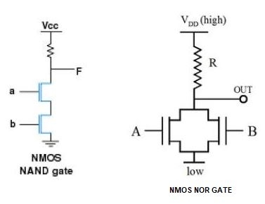
3. NAND and NOR with nMOS
| nMOS NAND | nMOS NOR |
|
When any input is ‘0’
|
When any input is ‘1’
|
|
When both inputs are ‘1’
|
When both inputs are ‘0’
|
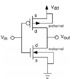
4. Complementary metal oxide semiconductor (CMOS)
- most widely used a family of large-scale devices combines high speed with low power consumption usually operates from a single supply of 5 – 15 V
- excellent noise immunity of about 30% of the supply voltage
- High fan-out: can be connected to a large number of gates (about 50)
- CMOS gates have equal no.of pMOS and nMOS
- CMOS inverter has a very high input resistance
CMOS inverter:
- Upper is pMOS, lower nMOS.
- When Vin = HIGH, Lower MOS on, VOUT =LOW
- When Vin = LOW, Upper MOS on, Vout = Vd = HIGH
Advantages of CMOS:
- This configuration greatly reduces power consumption since one of the transistors is always off in both logic states.
- Processing speed can also be improved due to the relatively low resistance compared to the nMOS-only or pMOS-only type devices.
- High Fan-out (usually 50)
- excellent noise immunity
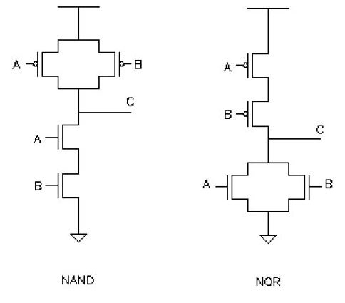
5. NAND and NOR with CMOS
| CMOS NAND | CMOS NOR |
|
If A=‘1’ and B=‘1’
|
If A=‘0’ and B=‘0’
|
|
If any A or B or both are ‘0’
|
If any A or B or both are ‘1’
|
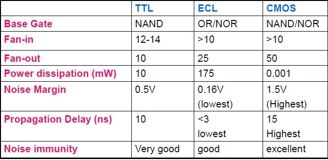
6. Logic families: Comparison
If you aiming to crack GATE & ESE, Other PSU Exams then you must try Online Classroom Program to get unlimited access to all the live structured courses and unlimited mock tests from the following links:
ESE and GATE EC Online Classroom Program (24+ LIVE Courses and 150+ Mock Tests)
Click on the Links Below to Avail Test Series:
Click Here Avail GATE/ESE EC Test Series !!! (150+ Mock Tests)
Thanks
Sahi Prep Hai To Life Set Hai!