- Home/
- GATE ELECTRONICS/
- GATE EC/
- Article
CMOS Inverter – Properties & Voltage Transfer Characteristics
By BYJU'S Exam Prep
Updated on: September 25th, 2023

The CMOS inverter plays an important role in all digital designs. CMOS inverter is abbreviated for Complementary Metal oxide semiconductor inverter. As we understand the operation and properties of the inverter clearly, designing intricate structures such as NAND gates, adders, multipliers, and microprocessors is greatly simplified.
In this article, we will focus on one single form of the inverter gate the Static CMOS Inverter. This is indeed the most popular inverter today and deserves special attention. The discussion will be around the basic idea of the CMOS Inverter, Switch model of the Inverter, Static Behavior, Voltage transfer characteristics, switching threshold, Noise Margin, and gain calculation.
Download Formulas for GATE Electronics & Communication Engineering – Control System
Table of content
What is the Basic Idea of a CMOS Inverter?
The basic structure of a Complementary Metal oxide semiconductor inverter consists of an n-MOS transistor and p-MOS transistor as a load and the gates of the two transistors are shorted at the input and the drains of the two transistors are also shorted where the output is obtained. The source n-MOS and p-MOS transistors of the CMOS Inverter are connected to the ground and supply respectively.
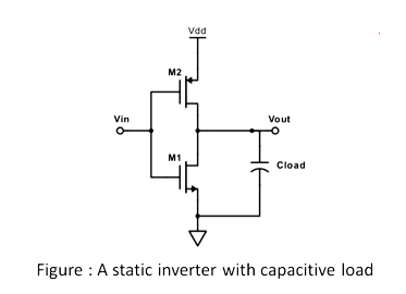
Its operation is readily understood with the help of the simple switch model of the MOS Transistor. The transistor is nothing more than a switch with an infinite off resistance (for| VGS|<|VT|) and a finite on-resistance (for |VGS|>|VT|). This leads to the following interpretation of the inverter.
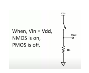
- When Vin is high and equal to VDD, the n-MOS transistor is ON while P-MOS is off. We get the following equivalent circuit where a direct path exists between Vout and the ground node, resulting in a steady-state value of 0V.
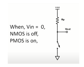
- On the other hand, when the input voltage is 0V, n-MOS and p-MOS transistors are OFF and ON respectively. The following equivalent shows that a path exists between VDD and Vout, yielding a high output Voltage.
Download Formulas for GATE Electronics & Communication Engineering – Digital Circuits
Properties of Static CMOS Inverter
A number of other important properties of static CMOS can be derived from the switch level view:
- Here High and low levels refer to VDD and grounds respectively. It means the voltage swing is the same as the voltage supply. This leads to a high noise margin.
- In steady-state, there always exists a path with finite resistance between the output and either VDD or GND. A properly designed CMOS inverter has a low output impedance, which makes it immune to noise and disturbances. Typical values of the output resistance are in the ‘k range’.
- The input impedance of the CMOS inverter is very high because the MOS transistor has silicon dioxide which behaves like an insulator and therefore, does not draw any dc input current. Since the input node of the inverter is connected to transistor gates, the steady-state input current is very near zero. A single inverter can theoretically drive an infinite number of gates (or have an infinite fan-out) and still be functionally operational; however, increasing the fan-out also increases the propagation delay. Although fan-out does not have any effect on the steady-state behaviour, it degrades the transient response.
- No direct path exists between the supply and ground rails under steady-state operating conditions (this is when the input and outputs remain constant). The absence of current flow (ignoring leakage currents) means that the gate does not consume any static power
Download Formulas for GATE Electronics & Communication Engineering – Electronic Devices
Voltage Transfer Characteristics(VTC) of CMOS Inverter
Transfer characteristics can be achieved by superimposing drain current-voltage characteristics of n-MOS and p-MOS transistors onto a common coordinate(Assuming VDD=2.5V).
![]()
Figure: Voltage Transfer Characteristics(VTC) of CMOS Inverter
|
Region |
Condition |
PMOS |
NMOS |
OUTPUT |
|
A |
0 |
Linear |
Cutoff |
V0=VDD |
|
B |
VTn |
Linear |
Saturation |
V0>VDD/2 |
|
C |
Vin=VDD/2 |
Saturation |
Saturation |
V0 drops sharply |
|
D |
VDD/2 |
Saturation |
Linear |
V0 |
|
E |
Vin>VDD-|VTp| |
Cut-off |
Linear |
V0=0 |
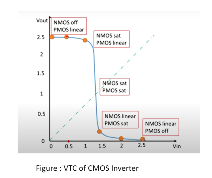
Switching Threshold of CMOS Inverter
- The switching threshold of VM can be obtained from the VTC graph where Vin=Vout.
- At this point, both transistors are in the saturation region.
- By ignoring channel modulation, we can equate the transistor currents.
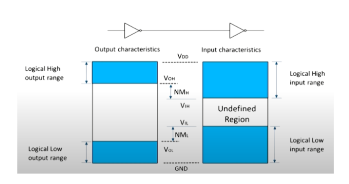
Noise Margin of CMOS Inverter
- The characteristics of an inverter define the allowable noise voltage on the input of the gate so that output will not be affected.
- The noise margin of an inverter is defined by
Noise Margin Low(NML) =VIL-VOL and Noise Margin High (NMH) =VOH-VIH
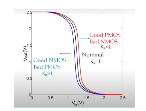
VTC with respect to process Variation Parameter
Where KR=Kn/Kp