- Home/
- GATE ELECTRONICS/
- GATE EC/
- Article
CMOS Fabrication Process – Types, Steps & Twin Tub Process
By BYJU'S Exam Prep
Updated on: September 25th, 2023

Today, CMOS Fabrication technology is the dominant IC fabrication technology in the VLSI industry and is used for making high-end microprocessors, microcontrollers, memory modules, sensors, and Application Specific Integrated Circuits (ASICs). The reasons for the dominant use of CMOS technology in the fabrication of VLSI chips are reliability, low power consumption, considerably low cost, and most importantly scalability. Earlier n-MOS technology was dominant but due to its major drawbacks such as its electrical symmetry and static power dissipation, all of these drawbacks can be minimized using CMOS Fabrication technology.
CMOS technology is one of the most important technologies in today’s VLSI. From the point of view of technology, in a CMOS Fabrication one can realize both a p-channel and n-channel MOSFET in various ways. In this article, we will discuss in detail all the steps involved in the CMOS fabrication process along with the types of processes involved.
Download Formulas for GATE Electronics & Communication Engineering – Control System
Table of content
What is the CMOS Fabrication Process?
CMOS which is also known as a complementary metal-oxide-semiconductor is a type of metal oxide semiconductor field-effect transistor (MOSFET) fabrication process that uses complementary and symmetrical pairs of p-type and n-type MOSFETs for logic functions.
CMOS technology is used for constructing integrated circuit (IC) chips, including microprocessors, microcontrollers, memory chips (including CMOS BIOS), and other digital logic circuits. CMOS technology is also used for analog circuits such as image sensors (CMOS sensors), data converters, RF circuits (RF CMOS), and highly integrated transceivers for many types of communication.
Download Formulas for GATE Electronics & Communication Engineering – Digital Circuits
What are Types of CMOS Fabrication Processes?
One can start with a p-type substrate and create an n-well or start with an n-type substrate and create a p-well or we can start with a very low doped substrate material nearly intrinsic and we can have both the wells which are called twin tub technology, twin well or twin tub. These are three different ways in which a CMOS can be realized. For n-MOS and p-MOS special region must be created in which the semiconductor type is opposite to the substrate type, these regions are called wells or tubs.
- n-tub Fabrication
- p-tub Fabrication
- Twin-tub Fabrication
Download Formulas for GATE Electronics & Communication Engineering – Electronic Devices
CMOS Fabrication Proces Steps
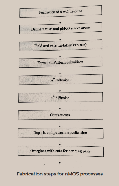
n-tub CMOS Fabrication circuits are superior to p-tub because of the lower substrate bias effect on transistor threshold voltage and inherently lower parasitic capacitances associated with the source and drain regions. The flow diagram of the fabrication for the nMOS process is illustrated in the figure below.
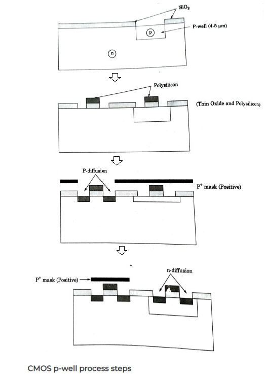
In this process of the p-tub CMOS fabrication, the structure consists of an n-type substrate in which p-type devices may be formed by suitable masking and diffusion. In order to accommodate n-type devices, a deep p-well is diffused into the n-type substrate as shown in the figure below.
The twin-tub process allows two separate tubs to be implanted into very lightly doped silicon. This allows the doping profiles in each tub region to be tailored independently so that neither type of device will suffer from excessive doping effects. The lightly doped silicon is an epitaxially grown layer on a heavily doped silicon substrate. The substrate can be either n-type or p-type. The process sequence for a CMOS twin-tub process is discussed as:
- The initial wafer is chosen n+ silicon and the initial wafer cleaning and back silicon implantation process takes place.
- Deposition of near intrinsic V-epitaxial wafer.
- Grow the nitride sandwich and etch. A reactive ion etching may be done to maintain a sharp edge definition. The nitride is left in the regions to become p-tub.
- Phosphors implanted as the n-tub dopant are at low energy and enter the exposed silicon but are masked from the adjacent region by the silicon nitride.
- The wafers are then selectively oxidized using the LOCOS method over the n-tub regions.
- The nitride is stripped and boron extras the silicon through the thin oxide but is masked from the n-tub by the thicker SiO2 layer. Intrinsic self-alignment has taken place in the entire process.
- Oxide is now stripped and a rapid steam oxide is grown. A separate anneal step is now incorporated. Drive-in the dopants takes place. During this drive-in, lateral diffusion of both n and p dopants takes place. Due to LOCOS, the silicon surface in the two tub regions is not the same and a link at the edge exists.
- After the tub formation, the formation of field oxide and gates is the same as that for the nMOS process.
- The threshold adjustment implants can be made into the channel regions of the devices to adjust the threshold voltages of the n and p channel transistors.
- The sources and drains are self-aligned to the gate. Selective implantation of the n-channel and p-channel source/drains to form n+ regions for the n-channels and implanted into all the sources and drains. This is followed by a selective implant of phosphorus or arsenic into the n-channel source/drain regions at a higher dose so that it over-compensates the bottom.
- After the subsequent thermal cycles, the phosphorus or arsenic completely covers the boron vertically and laterally.
- A phosphorus glass layer (PSG) is taken deposited and windows are etched.
- Aluminum metallization is defined using dry etching.
- The final layer is a plasma-deposited silicon nitride layer that seals the devices and provides mechanical scratch protection.
The twin-tub CMOS technology provides the basis for separate optimization of the p-type and n-type transistors.