
SR Flip-Flop: What is SR Flip-Flop Truth Table?
By BYJU'S Exam Prep
Updated on: September 25th, 2023

The SR Flip-Flop is also known as the gated or clocked SR latch. The clocked SR latch or SR flip-flop temporarily stores or holds the information until it is needed in digital circuits. ‘S’ and ‘R’ are the two inputs to the SR flip-flop. It has two outputs, the main output ‘Q’ and the complements of the main output ‘ Q’ ‘. The SR Flip-Flop is a storage element with only one bit.
The SR flip-flop is a gated SR flip-flop with a clock input circuitry that does not prevent the illegal or invalid output state that can arise when both inputs S and R are equal to logic level “1”. The SR latch is constructed using two cross-coupled NAND gates. Let us discuss in detail about these in the upcoming sections.
Download Complete Digital Logic Formula Notes PDF
Download Formulas for GATE Computer Science Engineering – Programming & Data Structures
Table of content
What is SR Flip-Flop?
The SR flip-flop is also named as RS flipflop. When both the inputs of the SR flip-flop are high, then the indeterminate state is theirs. In other programming environments, it is required to assign determinate outputs to all flipflop conditions. Hence, RS and SR flip-flops were designed. The clocked SR flip-flop is shown below.
Download Formulas for GATE Computer Science Engineering – Discrete Mathematics
SR Flip-Flop Circuit Diagram
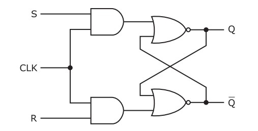
The circuit is similar to the SR latch except for the clock signal and two AND gates. The SR flip-flop circuit responds to the positive edge of the clock pulse to the inputs S and R.
SR Flip-Flop is Used as
SR Flip-Flop is Used as a storage device for a single data bit.
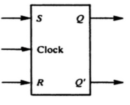
Symbol of SR Flip-Flop
The symbol of SR Flip Flop is shown below:
Download Formulas for GATE Computer Science Engineering – Algorithms
SR Flip-Flop Truth Table
‘S’ and ‘R’ are the two inputs to the SR flip-flop. The Qn represents the state of the SR flip-flop before applying the inputs, and Qn+1 represents the state of the SR flip-flop as output. The truth table for SR flip-flop is shown below:
| SR Flip-Flop Truth Table | ||||
|
Clock |
S |
R |
Qn+1 |
State |
|
0 |
X |
X |
Qn |
X |
|
1 |
0 |
0 |
Qn |
Hold |
|
1 |
0 |
1 |
0 |
Reset |
|
1 |
1 |
0 |
1 |
Set |
|
1 |
1 |
1 |
X |
Invalid |
SR Flip-Flop Characteristic Table
The characteristic table of SR flip-flop is as follows:
| SR Flip-Flop Characteristic Table | |||
|
S |
R |
Qn |
Qn+1 |
|
0 |
0 |
0 |
0 |
|
0 |
0 |
1 |
1 |
|
0 |
1 |
0 |
0 |
|
0 |
1 |
1 |
0 |
|
1 |
0 |
0 |
1 |
|
1 |
0 |
1 |
1 |
|
1 |
1 |
0 |
X |
|
1 |
1 |
1 |
X |
Characteristic Equation for SR Flip-Flop
The characteristic equation is an algebraic expression for the characteristic table’s binary information. It specifies the value of the next state of a flip-flop in terms of its present state and present excitation. To obtain the characteristic equation of SR flip-flop, the K-map for the next state Qn+1 in terms of present state and inputs is shown as:
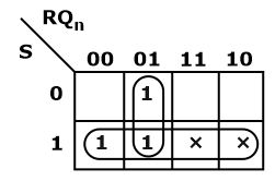
The characteristic equation of SR flip-flop from the above K-map is
![]()
Excitation Table of SR Flip-Flop
The truth table of flip-flop refers to the operation characteristic of the flip-flop. Still, in the designing of sequential circuits, we often face situations where the present state and the next state of the flip-flop are specified, and we must determine the input conditions that must exist in order for the intended output condition to occur.
The excitation table of SR flip-flop lists the present state, and the next state and the excitation table of SR flip-flop indicate the excitations required to take the flip-flop from the present state to the next state. The excitation table of SR flip-flops is as follows:
|
Qn |
Qn+1 |
S |
R |
|
0 |
0 |
0 |
X |
|
0 |
1 |
1 |
0 |
|
1 |
0 |
0 |
1 |
|
1 |
1 |
X |
0 |


