
NOR Gate Truth Table | Nor Gate Circuit Diagram
By BYJU'S Exam Prep
Updated on: September 25th, 2023

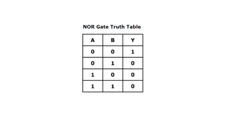
The NOR gate is a digital logic gate that implements logical NOR. A HIGH output (1) results if both the inputs to the gate are LOW (0); if one or both input is HIGH (1), a LOW output (0) results. NOR is the result of the negation of the OR operator.
The NAND gate and NOR gate are called Universal gates because they can perform all the three basic functions of AND, OR, and NOT gates. This article is about the NOR gate, its truth table, circuit diagram and other details.
Download Formulas for GATE Computer Science Engineering – Digital Logic
Table of content
What is NOR Gate?
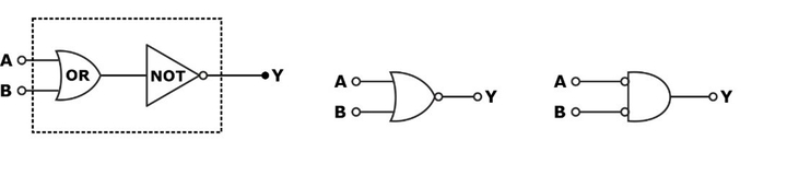
The NOR gate is one of the universal gates. A NOR gate combines an OR gate and a NOT gate. So we can say it is an OR-NOT operation. It may have two or more inputs and an output.
Download Formulas for GATE Computer Science Engineering – Computer Organization & Architecture
NOR Gate Symbol
The logical symbols of the NOR gate are shown:
NOR Gate Logical Expression
The logical expression for the output is
_ _ __
A + B = AB
It is clear from the truth table that the output is ‘1’ only if all the inputs are at logic ‘0’. It can also say that if the inputs A’ = B’ = 1, the output Y is 1. Thus, the NOR gate is equivalent to the AND gate with inverted inputs, and it can be realized by a bubbled AND gate, as shown above.
NOR Gate Truth Table
Download Formulas for GATE Computer Science Engineering – Operating Systems
Circuit Diagram of NOR Gate
- The NOR gate is also called the active LOW AND gate.
- The switching circuit of a NOR gate is as shown:
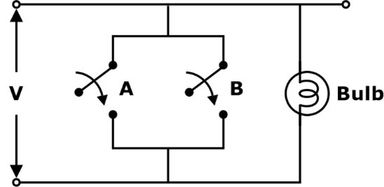
When any of the switches, either A or B, is closed, the bulb will not glow.
NOR gate follows the commutative law as follows:
___ ___
A+B = B+A
However, it does not follow the associative law.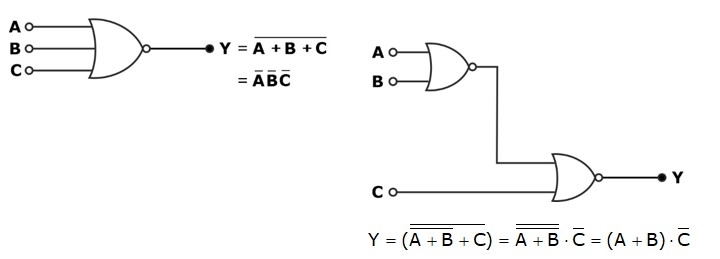
Enable and Disable Inputs
For a NOR Gate
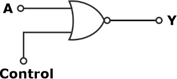
If control = 0;
|
A |
Control |
Y |
|
0 |
0 |
1 |
|
1 |
0 |
0 |
Thus, logic ‘0’ enables input.
If control = 1;
|
A |
Control |
Y |
|
0 |
1 |
0 |
|
1 |
1 |
0 |
Thus, logic ‘1’ is disabled input.
Realization of the Logic Gate – Using NAND Gate and NOR Gate
NOT Gate Realization
Using NOR gate
For the NOT gate realization, we require 1 NOR gate, as shown in the circuit diagram:

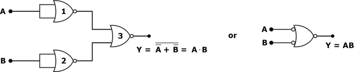
AND Gate Realization
Using NOR gate
For the AND gate realization, we require 3 NOR gates if the inputs are not available in complement form, as shown in the circuit diagram:
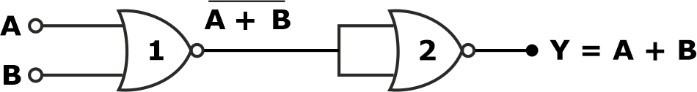
OR Gate Realization
Using NOR gate
For the OR gate realization, we require 2 NOR gates, as shown in the circuit diagram:
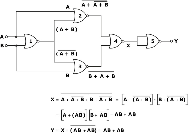
EX-OR Gate Realization
Using NOR gate
For the EX-OR gate realization, we require 5 NOR gates, as shown in the circuit diagram:
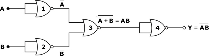
EX-NOR Gate Realization
Using NOR Gate
For the EX-NOR gate realization, we require 4 NOR gates, as shown in the circuit diagram: 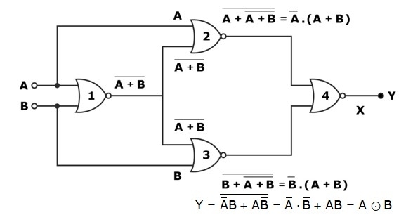
NOR Gate Realization Using NAND Gate
For the NOR gate realization using the NAND gate, we require 4 NAND gates, as shown in the circuit diagram:
Shortcuts for the realization of logic gates are as follows:
|
GATES |
Number of NOR gate |
|
NOT |
1 |
|
AND |
3 |
|
OR |
2 |
|
EX-OR |
5 |
|
EX-NOR |
4 |


