JK Flip Flop
By BYJU'S Exam Prep
Updated on: September 25th, 2023

JK Flip Flop is one of the most used flip-flops in digital circuits. The universal flip flop has two inputs, ‘J’ and ‘K.’ The JK Flip Flop is a gated SR Flip-Flop with a clock input circuitry that prevents the illegal or invalid output when both inputs S and R are equal to logic level “1.”
In the SR Flip-Flop, the ‘S’ and ‘R’ are the shortened abbreviated letters for the Set and Reset, but J and K are not. Instead, the J and K are autonomous letters chosen to distinguish the flip flop design from other types. Let us discuss in detail JK Flip-Flop in the upcoming sections.
Table of content
What is JK Flip-Flop?
The JK Flip-Flop is a refinement of the S-R flipflop in which the S-R type’s indeterminate (invalid) state is defined.
JK Flip-Flop Circuit Diagram
The logic diagram of JK Flip-Flop with data input J and K ed with O and Q respectively to obtain S and R inputs that is: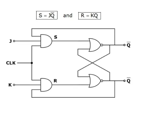
JK Flip-Flop Full Form
JK flip flop full form is Jack Kilby flip flop. It is named after its inventor Jack Kilby. They invented the integrated circuit in 1958.
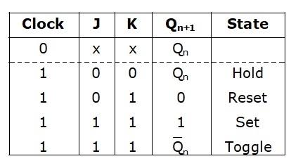
JK Flip-Flop Truth Table
The JK Flip-Flop truth table has the hold state, reset state, set state, and toggle state. As this is a refinement of SR flip flop, the truth table of SR flip flop is refined to make the truth table of jk flip flop. The truth table of the JK Flip-Flop has two inputs, J and K, Qn denotes the current state, and Qn+1 denotes the next state in the table given below:
Excitation Table of JK Flip-Flop
The excitation table of the JK Flip-Flop has the current state denoted by Qn, and the next state is denoted Qn+1. It has the J and K inputs for each transition in the excitation table of the JK Flip-Flop are as follows: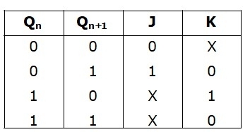
- Case-A: When, Qn = 0 and Qn+ 1 = 0
This condition can happen with either J = 0 and K = 0 or J = 0 and K = 1 (Characteristic table)
Therefore, the desired output Qn+1 = 0 is obtained when J= 0 and K= X (don’t care). - Case-B: When, Qn = 0 and Qn+ 1 = 1
This can happen with either J = 1 and K = 0 or J= 1 and K= 1 (toggle condition), which means in the toggle mode a jk flip-flop has J= 1 and K= 1.
Therefore the desired output Qn+ 1 = 1 is obtained when J= 1 and K=X (don’t care). - Case-C: When, Qn = 1 and Qn+ 1 = 0
This can happen with either J=0 and K= 1 or J= 1 and K=1. - Therefore, the desired output Qn+ 1 = 0 is obtained when J= X (don’t care) and K=1.
- Case-D: When, Qn = 1 and Qn+ 1 = 1
This condition can happen with either J= 0 and K= 0 or J= 1 and K=0.
Thus, the desired output Qn+ 1 = 1 is obtained with J = X and K=0.
Characteristic Table of JK Flip-Flop
The characteristic table of the JK Flip-Flop has the hold state, reset state, set state, and toggle state. The characteristic table has the input J and K, Qn and Qn+1 denote the current state denotes the next state in the characteristic table given below: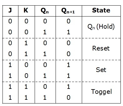
JK Flip-Flop Characteristic Equation
The characteristic equation of the JK Flip-Flop from the above characteristic table that has the hold state, reset state, set state, and toggle state is as follows using the three variable k-map. In the k-map, the column K’Qn is common, and the JQ’ is common. So, the characteristic equation is: 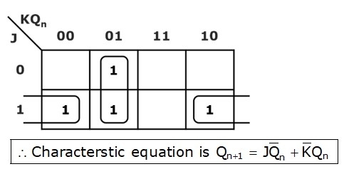
Also, check: Difference Between Flip-flop and Latch
Race Around Condition in JK Flip-Flop
The difficulty of both the inputs to be ‘1’ in the case of S-R of the invalid state is eliminated by a JK Flip-Flop using feedback connections from output to the input, as shown below. However, the condition when (level triggered) J = K = 1 is not yet perfect,
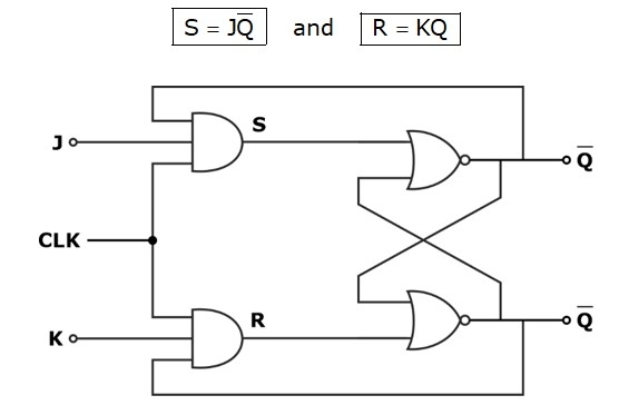
Consider J = K = 1 and Qn = 0 and a clock (CLK) is applied. After a propagation delay time tpd through two NAND gates, the output will toggle to Qn = 1. Since this is feedback to the inputs, the output will toggle back to Qn = 0 after another delay of tpd (FF).
Thus, as long as the clock pulse is present (tow), the output will toggle at every tpd(FF), and at the end of the clock pulse, the value of Qn is uncertain. This situation will continue as long as the low clock pulse width is longer than the flipflop propagation delay (tpd). Such a situation is referred to as the
ace around condition.
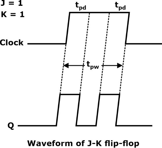
Thus, the Race around condition will occur when
(i) J = K = 1
(ii) When tpd (FF) < tpw
(iii) When the level trigger is applied.
One way to avoid this problem is to maintain tpw < Tpd(FF) < T. A most practical method for overcoming this problem is the use of the Master-slave configuration.
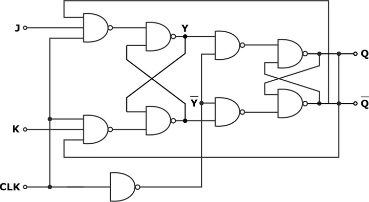
Master-Slave JK Flip-Flop
An M-S FF is constructed from 2 FFs (a MASTER and a SLAVE) and an ‘INVERTER.’
- On the rising edge of CLK (that is, +ve edge CLK PULSE), the control inputs are used to determine the output of the MASTER. When the CLK goes LOW (i.e., -ve edge CLK PULSE), the state of Master is transferred to the SLAVE, whose outputs are Q and Q.’
- In the M-S FF, the output is entirely dependent upon the output of SLAVE-FF.
Logic Diagram of Master-Slave JK Flip-Flop
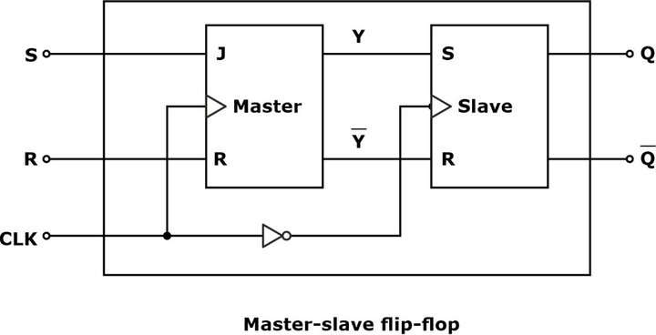
Operation
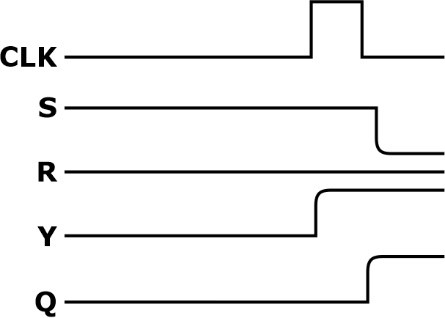
- When the clock pulse CLK is 0, the output of the inverter is 1. Since the clock input of the slave is 1, the flipflop is enabled, and output Q is equal to Y, while õ is equal to 7. The master flipflop is disabled because CLK = 0.
- When the pulse becomes 1, the information at the external R and S inputs is transmitted to the master Flip-Flop. In the slave flipflop, the clock is zero because the inverter output is zero. That is, a slave flipflop is isolated.
- When the pulse returns to the master flip-flop is isolated, preventing external inputs from affecting it. The slave flip-flop then goes to the same state as the master flip-flop.
Timing Diagram in M-S FF