
What is NAND Gate?
By BYJU'S Exam Prep
Updated on: September 25th, 2023

NAND Gate and NOR gate are called Universal gates because they can perform all the three basic functions of AND, OR, and NOT gates. Many logic gates are used to construct the digital system. A logic gate is a type of electronic circuit that has one or more inputs and one output.
A NAND gate with two inputs is a digital combination logic circuit that performs the logical inverse of an AND gate. In the NAND Gate truth table, while an AND gate only outputs a logical “1” if both inputs are logical “1,” a NAND gate outputs a logical “0” for the same input combination. The NAND gate truth table is provided in this article.
Download Formulas for GATE Computer Science Engineering – Digital Logic
Table of content
What is a NAND Gate?
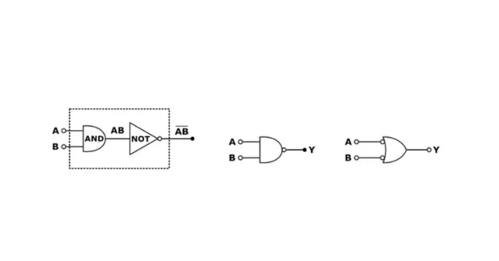
The NAND gate is a AND gate followed by a NOT gate. Thus, we can say it is a AND NOT operation. It may have two or more inputs but only one output.
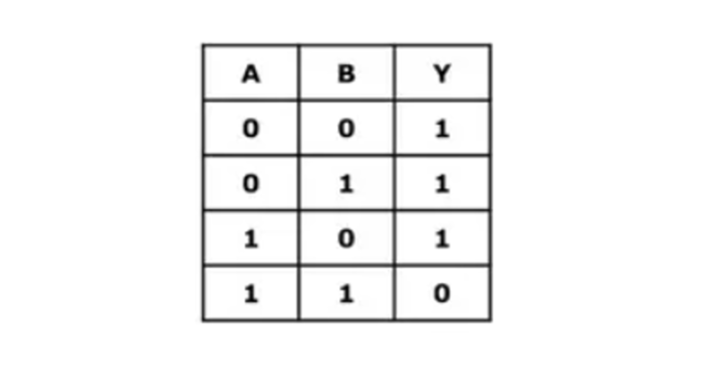
NAND Gate Truth Table
The truth table of NAND Gate is shown below:
NAND Gate Symbol
The logical symbols of the NAND gate are shown below:
NAND Gate Logical Expression
Thus, the logical expression for the output is:
__ ___ __ __
Y = A.B = A +B
Download Formulas for GATE Computer Science Engineering – Computer Organization & Architecture
NAND Gate Switching Diagram
It is clear from the NAND gate truth table of the two-input NAND gate that the output is 1 when either A or B or when both the inputs are at logic ‘0’. We can say that if Ā = 1 = B, both A and B are 1, and the output is 1. Therefore, the NAND gate can perform the OR function by inverting the inputs.
- The output is the exact inverse of the AND gate for all possible input combinations in the NAND gate.
- The OR gate with inverted inputs is called bubbled OR gate or negative OR gate. The NAND gate is also called an active low OR gate.
- The switching circuit diagram for a NAND gate is shown below.
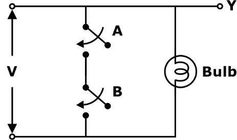
The bulb will glow when any of the switches A or B will open (logic 0).
- NAND gate follows the commutative law as (AB)’ = (BA).’
- NAND gate will not follow the associative law as
- Enable and disable inputs:
For a NAND Gate
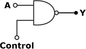
For control = 0;
|
A |
Control |
Y |
|
0 |
0 |
1 |
|
1 |
0 |
1 |
Thus, logic ‘0’ is the disabled input for the NAND gate.
For control = 1;
|
A |
Control |
Y |
|
0 |
1 |
1 |
|
1 |
1 |
0 |
Thus, logic ‘1’ is the enabled input for the NAND gate.
Download Formulas for GATE Computer Science Engineering – Operating Systems
Uses of NAND Gate
The NAND gate’s popularity is because it is the simplest of the digital logical operators to implement using transistor technology. This simple circuit was used to build the early microprocessors.
NAND gates detect a single low input in a digital system. A simple security system made up entirely of NAND gates. For example, the NAND gate monitors monitor the status of sensors connected to windows or doors. The sensor sends the security system a logical 1 signal when a window or door is closed. The alarm output is when all windows and doors are closed. When a single window or door is opened, the security system output changes to 1, which can be used to trigger an alarm or perform another action.
Advantages of NAND gate
NAND gates are low-cost devices with large storage capacities for their size. The NAND gate has good replaceability, which means that if the flash memory becomes damaged, it can be replaced with an appropriate component.
NAND gate memory capacity can replace large files such as USB drives, digital cameras, and tablets. The NAND gate has extreme endurance and durability.
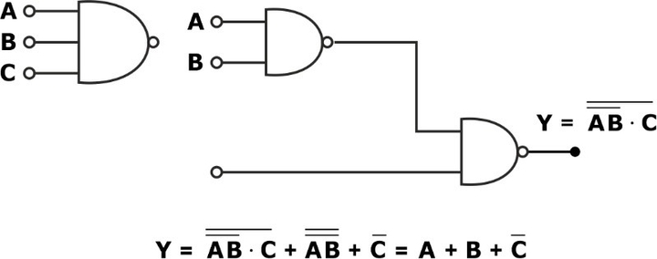
Realization of the Logic Gate Using NAND Gate
In Boolean Algebra, the NAND gate is called a universal gate because any digital circuit can be implemented by using any one of these two i.e. any logic gate can be created using NAND gate.
NOT Gate Realization
For the NOT gate realization, we require 1 NAND gate as shown in the circuit diagram:

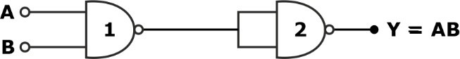
AND Gate Realization
For the AND gate realization, we require 2 NAND gates, as shown in the circuit diagram:
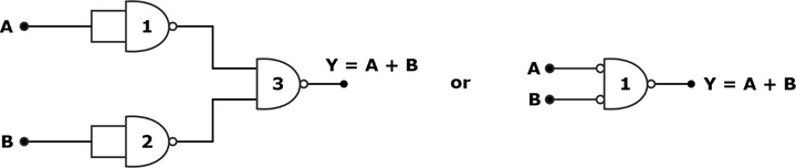
OR Gate Realization
For the OR gate realization, we require 3 NAND gates if the inputs are not available in complement form, as shown in the circuit diagram:
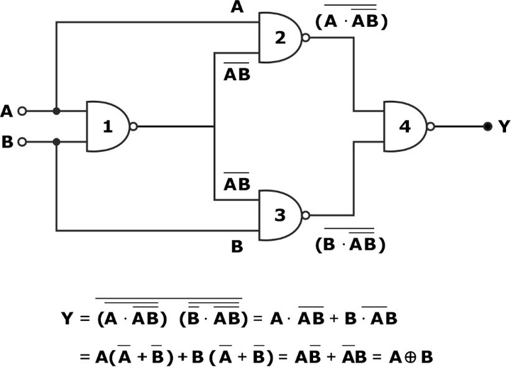
EX-OR Gate Realization
For the EX-OR gate realization, we require 4 NAND gates, as shown in the circuit diagram:
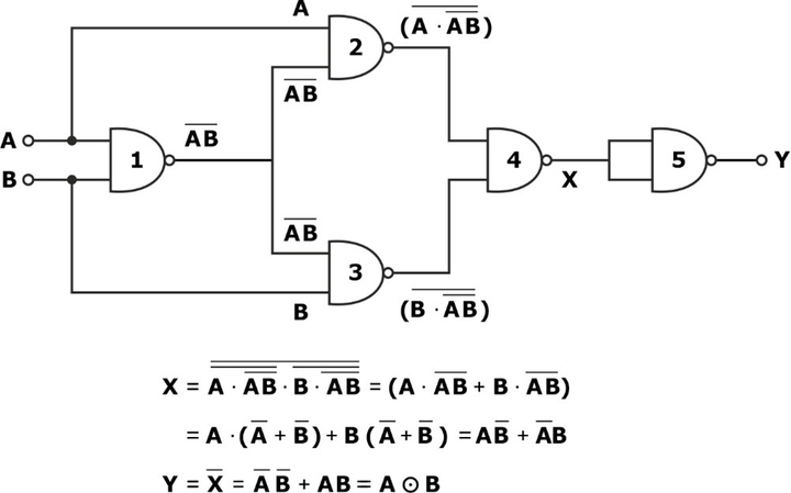
EX-NOR Gate Realization
For the EX-NOR gate realization, we require 5 NAND gates, as shown in the circuit diagram:
Shortcuts for the realization of logic gates are as follows:
|
GATES |
Number of NAND Gate |
|
NOT |
1 |
|
AND |
2 |
|
OR |
3 |
|
EX-OR |
4 |
|
EX-NOR |
5 |


