This article covers the study notes on Basics Electronics Engineering-II which include topics such as Operational Amplifiers, Integrated Circuits and Optoelectronic Devices.
Operational Amplifiers
- Op-Amp (Operational Amplifier) is a fundamental building block for handling analog electrical signals.
- An operational amplifier is a high gain, differential, voltage amplifier.
- OP AMP has two inputs called “+” and “-,” ( or VIN+ and VIN-) and a single output.
- The output depends only on the difference of the voltage on the two inputs.
- If the difference of the two input voltages is VIN , the output voltage is VOut, then VOut = ΔVIN GV; where Gv is the (voltage) gain.
- Differential operation involves the use of opposite polarity inputs.
- Common mode operation involves the use of the same polarity inputs.
- Common-mode rejection compares the gain for differential inputs to that for common inputs.


- An ideal op-amp is usually considered the following properties, and they are considered to hold for any input voltages:
- Infinite open loop gain
- Infinite bandwidth ( the frequency magnitude response is flat everywhere with zero phase shift)
- Infinite input impedance
- Zero input current (There is no leakage or bias current into the device)
- Zero input offset voltage (when the input terminals are shorted, output is a virtual ground)
- Infinite slew rate (Rate of change of the output voltage is unbounded) and power bandwidth (full output voltage and current available at all frequencies).
- Zero output impedance (Rout = 0, and so output voltage does not vary with output current)
- Zero noise
- Infinite CMRR (Common mode rejection ratio)
- Infinite Power supply rejection ratio for both power supply rails.
Properties of Op-Amp  Op-Amp Classification
Differential Operational Amplifier:
- A differential operational amplifier has inverting and non-inverting inputs with high input impedance and differential or open-loop gains between 1000 and 10 million.
- When the inverting input is used with negative feedback due to R0, the closed loop gain is given by (-R0 / R1) and the input impedance is R1 the output impedance is the open loop output impedance divided by loop gain.

or
Loop gain (dB) = Open loop gain (dB) – Closed loop gain (dB)
- If a number of signals are connected to the inverting input, the output is proportional to the sum of the input signals, making possible the solution of linear algebraic and differential equations on an analog computer.
- If the non-inverting input to a differential operational amplifier is used, the input impedance is increased to a value,
Rcm || (Ri × loop gain)
where Rcm is the common mode impedance and Ri is the differential impedance.
- One way to increase input impedance to an amplifier utilizing the inverting input is to reduce the feedback voltage by connecting a voltage divider at the output.
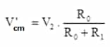
- The voltage gain for a non-inverting input is:
- A true ideal differential amplifier the difference between two input voltages providing an output,

- In practice, the output also consists of an error term that is due to the common-mode input voltage = (V1 + V2)/2.
- Total output of a differential amplifier is:

Common Mode Rejection Ratio (CMRR)
- The common mode rejection ratio is a figure of merit of a differential amplifier, since it is the ratio of differential gain, Ad (the desired gain), to the common-mode gain AC.
![]()
or
![]()
- Emitter-coupled differential amplifiers are the type of circuit used predominantly in ICs, because of the manufacturing ability to closely match components, and since the devices are so closely spaced their variations due to temperature tend to cancel, providing excellent DC coupling stability.
- High values of CMRR are provided by large effective values of emitter resistance Re, in the emitter-coupled amplifier. This may be provided by a transistor or CRD to provide essentially a constant-current source in the emitter.
![]()
Ideal Voltage Transfer Curve:
- The graphic representation of the output equation is shown in figure in which the output voltage V0 is plotted against differential input voltage Vd, keeping gain Ad constant.

Non-linear Op-Amp Circuits
Integrator- Circuit Diagram

- Output Voltage
- Circuit Diagram

- Output Voltage
- Circuit Diagram

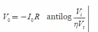
- Output Voltage:
- η= recombination factor, Vt= thermal voltage, and I0= reverse saturation current of diode.
- Circuit Diagram

- Output Voltage
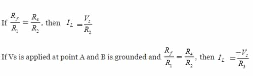
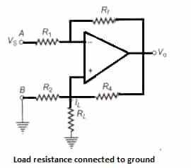
Determination of Grounded Load
Capacitance Multiplier


- Equivalent capacitance:

- This circuit is useful in creating artificially large values of capacitances while using low-valued C which is normally available.
Inductance Simulator

![]()
- Inductance Leq=CR1R2 Henry
- Quality factor:

Non-inverting Integrator
- The circuit shown below is a non-inverting integrator, where negative feedback exists.
- The analysis will be as follows.
![]()
or ![]()

Non-inverting Differentiator
- It uses a single operational amplifier.
- The main feature of the circuit is that the input impedance is purely resistive.
![]()
or
![]()

Applications of Operational amplifiers:
- Inverting Amplifier
- Non-inverting Amplifier
- Differentiator
- Differential Amplifier
- Voltage follower
- Selective inversion circuit
- Current-to-voltage converter
- Active rectifier
- Integrator
- Comparator
- Filters
- Voltage comparator
- Signal Amplifier
Integrated Circuits
Introduction
- Integrated circuits compose the major portion of the field of microelectronics and may consist of film, monolithic or hybrid circuits.
- A monolithic IC consists of active and passive components formed by diffusion into a single silicon chip, with interconnection provided by an aluminium metallization process.
- Silicon is a semiconductor with resistance between that of conductor and an insulator.
- The conductivity of silicon can be changed several orders of magnitude by introducing impurity atoms in silicon crystal lattice.
Fabrication Steps
The monolithic fabrication process consists of wafer preparation, epitaxial growth, diffused isolation, base and emitter diffusions, pre-ohmic etch, metallization, circuit probing, dicing, mounting and packaging, wire bonding, encapsulation and final testing.
- Each diffusion process involves such as items silicon dioxide layer, photo resist mask, ultraviolet exposure, etching, scrubbing and diffusion.
- Practical IC resistance values obtainable range from 25 Ω to 500 k Ω, depending upon the sheet resistivities measured in ohms per square. p-type diffused resistors have values from 50 to 250 Ω per square and pinch resistors have a value of 5000 Q per square.
- Because the tolerances of resistance values are at best ±30%, ICs are designed to utilize resistance ratios, which may be controlled to within 3%.
- Capacitors may be obtained by utilising the p-n junctions in transistor type structures or the MOS capacitive effects employing the silicon-dioxide layer. Practical values range from 3 to 30 pF because of the excessive area used for larger values.
- By suitable interconnecting COS/MOS ICs, an inverter circuit with very low quiescent dissipation can be made available, and by further interconnections of many inverters, many of the logic gates found in digital systems may be implemented.
- Integrated circuits may be of the monolithic or hybrid type, with the latter being a mixture of thin-film and diffused components.
- Complementary Symmetry MOS ICs (COS/MOS) involves both a p-channel and an n-channel MOSFET fabricated on the same chip.
- Large Scale Integration (LSI) involves the fabrication of 100 or more logic gates on a single chip, while Medium Scale Integration (MSI) is defined as more than 12 but less than 100 gates on a single chip.
Fabrication Process
The fabrication of integrated circuits consists basically of the following process steps:
- Lithography: The process for pattern definition by applying a thin uniform layer of viscous liquid (photo-resist) on the wafer surface. The photoresist is hardened by baking and then selectively removed by the projection of light through a reticle containing mask information.
- Etching: Selectively removing unwanted material from the surface of the wafer. The pattern of the photoresist is transferred to the wafer by means of etching agents.
- Deposition: Films of the various materials are applied on the wafer. For this purpose mostly two kinds of processes are used, physical vapour deposition (PVD) and chemical vapour deposition (CVD).
- Chemical Mechanical Polishing: A planarization technique by applying chemical slurry with etchant agents to the wafer surface.
- Oxidation: In the oxidation process oxygen (dry oxidation) or H2O (wet oxidation) molecules convert silicon layers on top of the wafer to silicon dioxide.
- Ion Implantation: Most widely used technique to introduce dopant impurities into the semiconductor. The ionized particles are accelerated through an electrical field and targeted at the semiconductor wafer.
- Diffusion: A diffusion step following ion implantation is used to anneal bombardment-induced lattice defects.
Oxidation:
- It is a process which converts silicon on the wafer into silicon dioxide.
- The chemical reaction of silicon and oxygen already starts at room temperature but stops after a very thin native oxide film.
- For an effective oxidation rate, the wafer must be settled to a furnace with oxygen or water vapour at elevated temperatures.
- Silicon dioxide layers are used as high-quality insulators or masks for ion implantation.
- The ability of silicon is to form high-quality silicon dioxide.
Diffusion:
- Diffusion is the movement of impurity atoms in a semiconductor material at high temperatures.
- The driving force of diffusion is the concentration gradient.
- There is a wide range of diffusivities for the various dopant species, which depend on how easy the respective dopant impurity can move through the material.
- Diffusion is applied to anneal the crystal defects after ion implantation or to introduce dopant atoms into silicon from a chemical vapour source.
- In the last case, the diffusion time and temperature determine the depth of dopant penetration.
- Diffusion is used to form the source, drain, and channel regions in an MOS transistor.
- But diffusion can also be an unwanted parasitic effect because it takes place during all high-temperature process steps.
Ion Implantation:
- Ion Implantation is the process of adding impurities to a silicon wafer.
- This is performed with an electric field which accelerates the ionized atoms or molecules so that these particles penetrate into the target material until they come to rest because of interactions with the silicon atoms.
- Ion implantation is able to control exactly the distribution and dose of the dopants in silicon because the penetration depth depends on the kinetic energy of the ions which is proportional to the electric field. The dopant dose can be controlled by varying the ion source.
- Unfortunately, after ion implantation, the crystal structure is damaged this implies worse electrical properties.
- Another problem is that the implanted dopants are electrically inactive because they are situated on interstitial sites.
- Therefore after ion implantation, a thermal process step is necessary which repairs the crystal damage and activates the dopants.
Photolithography:
- Lithography is used to transfer a pattern from a photomask to the surface of the wafer.
- Photolithography is the process of creating patterns on a smooth surface (Silicon wafer).
- This is accomplished by selectively exposing parts of the wafer while other parts are protected. The exposed sections are susceptible to doping, removal, or metallization. Specific patterns can be created to form regions of conductors, insulators, or doping. Putting these patterns onto a wafer is called photolithography.
- The pattern defined by the mask is either removed or remained after development, depending if the type of resist is positive or negative.
Etching:
- Etching is used to remove material selectively in order to create patterns.
- The pattern is defined by the etching mask, because the parts of the material, which should remain, are protected by the mask.
- The unmasked material can be removed either by wet (chemical) or dry (physical) etching.
Twin-tub CMOS process
- It is also possible to create both a p-well and an n-well for the n-MOSFET's and p-MOSFET respectively in the twin well or twin tub technology. Such a choice means that the process is independent of the dopant type of the starting substrate (provided it is only lightly doped).

- Provide separate optimization of the n-type and p-type transistors.
- It is possible for threshold voltage, body effect and the channel transconductance of both types of transistors to be tuned independently.
- Generally, the starting material is a p+ or n+ substrate, with a lightly doped epitaxial layer on top. This epitaxial layer provides the actual substrate on which the n-well and the p-well are formed.
- Since two independent doping steps are performed for the creation of the well regions, the dopant concentrations can be carefully optimized to produce the desired device characteristics.
Optoelectronic Devices
Optoelectronic Devices
Modern solid state devices, which include emitters, sensors and collectors, usually are known as optical electronic devices or optoelectronics.
- The radiations from a tungsten lamp is mostly in the infrared region, with relatively little in the visible region. It is often used as a source of infrared radiation.
- Illumination is a measure of the visible radiation on a surface and is measured in foot candles or lumens/sq-ft.
- Irradiance is a measure of the total radiation on a surface and is measured in watt/cm2.
Light Absorption and Emission: Light absorption and emission in a semiconductor is known to be heavily dependent on the detailed band structure of the semiconductor.
Direct Bandgap Semiconductors: Direct bandgap semiconductors, i.e., semiconductors for which the minimum of the conduction band occurs at the same wave vector k, as the maximum of the valence band, have a stronger absorption of light as characterized by a larger absorption coefficient.
Indirect Bandgap Semiconductors: Indirect bandgap semiconductors, i.e., semiconductors for which the minimum of the conduction band does not occur at the same wave vector as the maximum of the valence band, are known to have a smaller absorption coefficient and are rarely used in light emitting devices.

Photo-diode: The photo conductors which are junction type, are photo-diodes or photo transistors where in one or more p-n junction are used under reverse bias. Electron hole pairs resulting from photons incident on the p-n junction add to the minority carriers due to the reverse bias.

Note: Silicon and germanium photo sensors have their peak spectral response in the infrared region, with their response in the visible only approximately 40% of maximum.
- The inherent current gain of a transistor provides the photo transistor with a high current gain in the region of 1 mA/mW/cm2.
- By adding a second conventional transistor, a photo Darlington amplifier results, with even higher sensitivity.
- Photo-diodes and photo transistors may be operated as switching devices in light-operated relays, shaft encoders, paper tape readers, brush less DC motors, etc.
Variations of the basic p-n photo-diode are
- PIN photo-diode (Ultrafast response),
- Avalanche photo-diode (Higher current sensitivity and fast response),
- Photo-diode (Inexpensive higher current sensitivity but slower response)
Photovoltaic Sensors: Photovoltaic sensors, usually either silicon or selenium, generate a voltage under open circuit conditions of typically 0.5V. When operated in the short-circuit mode, the current is proportional to the illumination and can be used to provide a direct reading foot-candle metre. Photovoltaic sensors may be series parallel interconnected to provide large area solar power cells.
Light Emitting Diodes (LEDs): It is a special type of p-n junction device that under forward conditions can emit external spontaneous radiation in ultraviolet, visible and infrared regions of electromagnetic spectrum. Light Emitting Diodes may emit visible radiation when the p-n junction is diffused in GaAsP, infrared if constructed from GaAs, and a laser beam if sufficiently highly pulsed current is applied to a GaAs junction. A popular alphanumeric display is the LED seven segment device, which can provide high brightness for only a few milliwatts of input power per segment.

Photovoltaic (Solar Cells): The solar cells are semiconductor junction devices which are used for converting optical radiation (sunlight) into electrical energy. The generated electric voltage is proportional to the intensity of incident light. Due to their capability of generating voltage they are called as photovoltaic cells. p-n junction solar cells are currently used to supply electrical power for many space satellites.
When a photon of light energy collides with the valence electron either in p-type material or n-type material, it imparts sufficient energy to the electron to leave its parent atom. As a result, free electrons and holes are generated on each side of the junction. In p-type material, the newly generated electrons are minority carriers.

These electrons move freely across the junction with no applied bias. Similarly, in n-type material, the newly, generated holes are minority carriers
These holes move freely across the junction with no applied bias. The result is an increase in minority carrier flow. In this way, depletion region potential causes the photo current to flow through the external load.
- The solar cell is self generating device i.e., it does not require any external power source.
- The internal emf and current generated by solar cell is enough which can be measured by galvanometer.
- Solar cell can't convert all solar radiation into electric energy.
All the Best.
Team gradeup!


Comments
write a comment