- Home/
- GATE ELECTRICAL/
- GATE EE/
- Article
Revision Notes for Analog Circuits: GATE EE Champion Study plan 2022
By BYJU'S Exam Prep
Updated on: September 25th, 2023

Revision Notes for Analog Circuits GATE EE Champion Study plan 2022: The related notes and quizzes are available which have been released throughout the preparation of the subject with some other useful articles. This article would be a handful for the future when the whole syllabus would be completed and the revision period of the subject would be going on. Aspiring Candidates can get benefit from this article and boost their preparation with an ongoing champion Study plan for GATE EE 2022.
Table of content
Brief Introduction about a topic
Logic Gates
- AND Gate:

If one of the inputs A or B is grounded, current flows through the diode and the output node C is at a low voltage. The only way to get a high output is by having both inputs high. This circuit is equivalent to logical AND function.
- OR Gate:

If one or both of the inputs A and B are high, current flows through the associated diode and the output node C at a high voltage. It is equivalent to OR Gate.
Clipper Circuits
A Diode network that has the ability to clip a portion of the input signal without distorting the remaining part of the alternating waveform is known as Clipper.
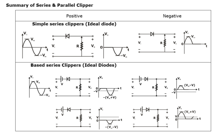
There are two general categories of clippers
- Series clipper
- Parallel Clipper
The series configuration is defined as one where the diode is in series with the load, while the parallel configuration has the diode in a branch parallel to the load.
Series Clipper:
- Unbiased Clipper
The response of the series configuration of figure 1(a) to a variety of alternating waveforms is provided in figure 1(b)
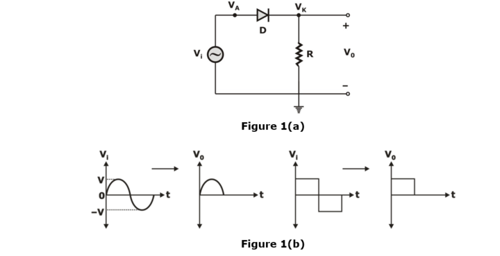
From figure 1(a), Anode voltage of diode VA = Vi and Cathode voltage VK = 0
Therefore, for positive half cycle VA > VK, which means diode is forward biased and act as short circuit.
For negative half cycle VA < VK, which means diode is reverse biased and act as open circuits.
- Biased clipper
The addition of a dc supply that can have a pronounced effect on the output of a clipper is shown in figure 2.
NOTE: Make a mental sketch of the response of the network based on the direction of the diode and the applied voltage levels.
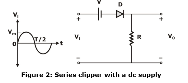
For the given network, the direction of the diode suggests that the signal Vi must be positive to turn it ON. The dc supply further requires that the voltage Vi be greater than V to turn ON the diode. The negative region of the input signal is pressuring the diode into the OFF state, supported further by the dc supply.
NOTE: Determine the applied voltage (transition voltage) that will cause a change in state for the diode.
For the ideal diode, the transition between states will occur on the characteristics, where Vd = 0 V and id = 0A. Applying the condition id = 0 at Vd = 0 to the network of figure 2 will result in the configuration of figure 3(a), where it is recognized that the level of Vi that will cause a transition in the state is Vi = V
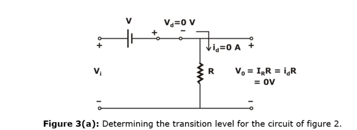
For an input voltage greater than V volts the diode is in the short circuit state, while input voltage less than V volts it is in the open circuit or off state.
NOTE: Be continually aware of the defined terminals and polarity of V0.
When the diode is in the short circuit state, such as shown in figure 4, the output voltage V0 can be determined by applying KVL in the clockwise direction.
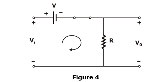
Vi – V – V0 = 0
∴ V0 = Vi – V
NOTE: It can be helpful to sketch the input signal above the output and determine the output and determine the output at instantaneous values of the input.
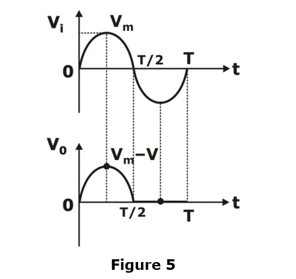
For an instantaneous value of Vi, the input can be treated as a dc supply of that value and the corresponding dc value of the output determined.
For instant at Vi = Vm
For Vm > V, the diode is short circuit and V0 = Vm – V
When diode change state, and Vi = – Vm
Then V0 = 0 V
And now complete the curve for V0 that can be shown in figure 5.
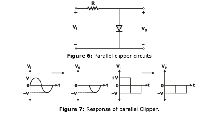
Parallel Clipper:
The network of figure 6 is the simplest parallel diode configuration with the output for the same input as discussed earlier. The analysis of parallel configuration is very similar to that applied to series configurations.
Clampers
The clamping network is one that will clamp a signal to a different dc level. The network consists of a capacitor, a diode and a resistor element and an independent dc supply to introduce on additional shift.
The magnitude of R and C must be chosen such that the time constant τ = RC is large enough to ensure that the voltage across the capacitor does not discharge significantly during the interval the diode is nonconducting.
There is basically two types of clamper:
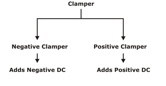
Negative Clamper:
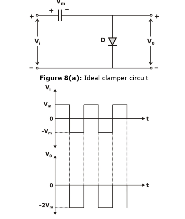
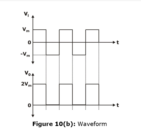
Figure 8(b): Waveform
When the input is positive, the diode operates in forwarding bias and capacitor charge through the diode. If the diode is ideal it behaves as a short circuit and therefore capacitor charge up to the peak input Vm.
When input becomes negative, the capacitor should discharge but the discharge path is not available so the capacitor voltage will continue to remain Vm. Therefore, once the capacitor is fully charged its voltage Vm irrespective of the input being positive or negative.
Applying KVL
–Vi + Vm + V0 = 0
V0 = Vi – Vm
= Vi + (– Vm)
Hence circuit adds a dc voltage of –Vm. So, the output will be a square waveform for given input whose value varies from 0 to – 2Vm.
The positive peak of the output waveform touches the 0V level or the positive peak gets clamped to 0V. Since a negative clamper is clamping positive peak to 0V so it is called a positive peak clamper.
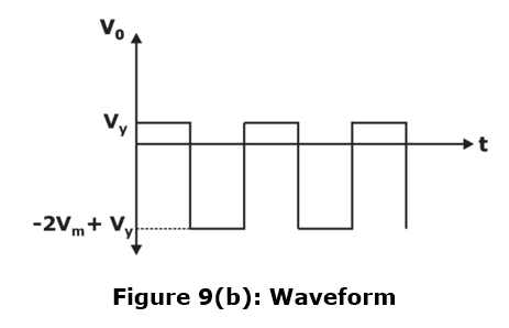
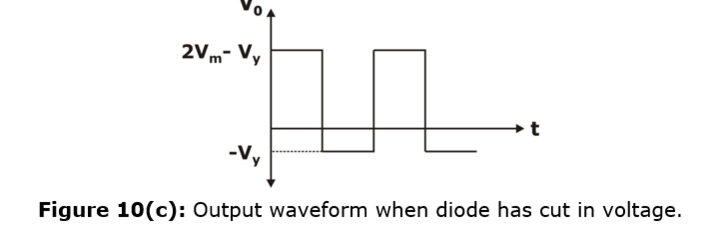
NOTE: If the diode has cut in voltage Vγ then it should be replaced with a series connection of the ideal diode and battery Vγ.
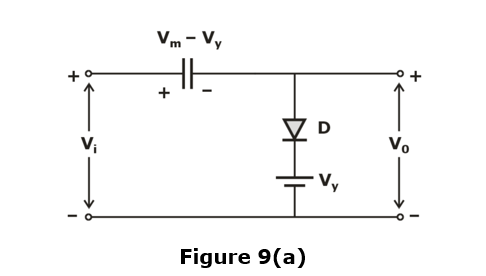
When input is +Ve, capacitor changes through diode upto a maximum voltage of Vm – Vγ
∴ V0 = Vi = (Vm – Vγ)
V0 = Vi + (–Vm + Vγ)
Hence circuit add dc voltage equal to – (Vm – Vγ)
Positive Clamper:
- When the input is negative diode gets forward biased and capacitor charges through diode up to peak input Vm
- When input becomes positive capacitor will not be able to discharge as the discharge path is not present. Therefore, the voltage across the capacitor remains Vm irrespective of input being +Vm or –Vm
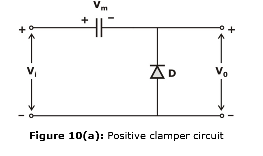
Applying KVL
V0 = Vi + Vm
Negative peak output gets clamped to 0 volts therefore positive clamper is also called negative clamper.
NOTE: It diode has cut in voltage Vγ then capacitor charges to a voltage (Vm – Vγ)
∴ V0 = Vi + (Vm – Vγ)
Hence added dc voltage is Vm – Vγ
Example:
In the circuit shown in figure dc value at the output is?
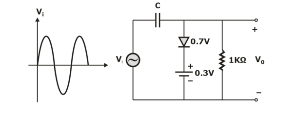
Solution:
For the given clamper circuit, make diode short and calculate maximum voltage across capacitor.
– Vi + VC = 0.7V + 0.3 = 0
VC = Vi – 1 = 5 – 1
= 4V
Now, make diode open circuit
– Vi + VC + V0 = 0
V0 = Vi – VC
= Vi – 4V
Dc value of output = –4V
Notes for Analog Circuits
Here we provide all related notes for Analog Circuits which have been released throughout the preparation. The six days schedule is as follows:
- Day 1
- Day 2
- Day 3
- Day 4
- Day 5 & 6
Quizzes for Analog Circuits:
- GATE 2022 Analog Electronics Quiz 1
- GATE 2022 Analog Electronics Quiz 2
- GATE 2022 Analog Electronics Quiz 3
- GATE 2022 Analog Electronics Quiz 4
- GATE 2022 Analog Electronics Quiz 5
- GATE 2022 Analog Electronics Quiz 6
Other useful Articles:
- Best books for Analog Circuits
- Important Topics for Analog Circuits
- Important Formulas for Analog Circuits
- Weightage Analysis for Analog Circuits
| Important Related Links | |
Thanks
Sahi Prep hai to Life Set Hai !!