EDC & Analog Electronics : Diode Types & its Applications
Clipper Circuits
Diode network that have the ability to clip of a portion of the input signal without distorting the remaining part of the alternating waveform is known as Clipper.
There are two general categories of clippers
- Series clipper
- Parallel Clipper
The series configuration is defined as one where the diode is in series with the load, while the parallel configuration has the diode in a branch parallel to the load.
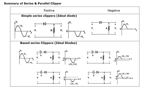
(a) Series Clipper
(i) Unbiased Clipper
The response of series configuration of figure 1(a) to a variety of alternating waveform is provided in figure 1(b)

From figure 1(a), Anode voltage of diode VA = Vi and Cathode voltage VK = 0
Therefore, for positive half cycle VA > VK, which means diode is forward biased and act as short circuit.
For negative half cycle VA < VK, which means diode is reverse biased and act as open circuits.
(ii) Biased clipper
The addition of a dc supply that can have a pronounced effect on the output of a clipper is shown in figure 2.
NOTE: Make a mental sketch of the response of the network based on the direction of the diode and the applied voltage levels.

For the given network, the direction of diode suggest that the signal Vi must be positive to turn it ON. The dc supply further requires that the voltage Vi be greater than V to turn ON the diode. The negative region of the input signal is pressuring the diode into the OFF state, supported further by the dc supply.
NOTE: Determine the applied voltage (transition voltage) that will cause a change in state for the diode.
For the ideal diode the transition between states will occur on the characteristics, where Vd = 0 V and id = 0A. Applying the condition id = 0 at Vd = 0 to the network of figure 2 will result in the configuration of figure 3(a), where it is recognized that the level of Vi that will cause a transition in state is Vi = V

For an input voltage greater than V volts the diode is in the short circuit state, while input voltage less than V volts it is in the open circuit or off state.
NOTE: Be continually aware of the defined terminals and polarity of V0.
When the diode is in the short circuit state, such as shown in figure 4, the output voltage V0 can be determined by applying KVL in the clockwise direction.

Vi – V – V0 = 0
∴ V0 = Vi – V
NOTE: It can be helpful to sketch the input signal above the output and determine the output and determine the output at instantaneous values of the input.

For an instantaneous value of Vi the input can be treated as a dc supply of that value and corresponding dc value of the output determined.
For instant at Vi = Vm
For Vm > V, diode is short circuit and V0 = Vm – V
When diode change state, and Vi = – Vm
Then V0 = 0 V
And now complete the curve for V0 that can be shown in figure 5.
(b) Parallel Clipper
The network of figure 6 is the simplest of parallel diode configuration with the output for the same input as discussed earlier. The analysis of parallel configuration is very similar to that applied to series configurations.

Clampers
The clamping network is one that will clamp a signal to a different dc level. The network consist of a capacitor, a diode and a resistor element and an independent dc supply to introduce on additional shift.
The magnitude of R and C must be chosen such that the time constant τ = RC is large enough to ensure that the voltage across the capacitor does not discharge significantly during the interval the diode is non conducting.
There are basically two type of clamper:

(a) Negative Clamper

Figure 8(b): Waveform
When the input is positive, diode operates in forward bias and capacitor charge through diode. If diode is ideal it behaves as short circuit and therefore capacitor charge up to the peak input Vm.
When input becomes negative, capacitor should discharge but discharge path is not available so capacitor voltage will continue to remain Vm. Therefore, once capacitor is fully charged its voltage Vm irrespective of the input being positive or negative.
Applying KVL
–Vi + Vm + V0 = 0
V0 = Vi – Vm
= Vi + (– Vm)
Hence circuit adds dc voltage of –Vm. So, the output will be a square waveform for given input whose value varies from 0 to – 2Vm.
Positive peak of output waveform touches 0V level or positive peak gets clamped to 0V. Since a negative clamper is clamping positive peak to 0V so it is called positive peak clamper.
NOTE: If diode has cut in voltage Vγ then it should be replaced with series connection of ideal diode and battery Vγ.

When input is +Ve, capacitor changes through diode upto a maximum voltage of Vm – Vγ
∴ V0 = Vi = (Vm – Vγ)
V0 = Vi + (–Vm + Vγ)
Hence circuit add dc voltage equal to – (Vm – Vγ)

(b) Positive Clamper
- When input is negative diode gets forward biased and capacitor charges through diode up to peak input Vm
- When input becomes positive capacitor will not be able to discharge as discharge path is not present. Therefore, voltage across the capacitor remains Vm irrespective of input being +Vm or –Vm

Applying KVL
V0 = Vi + Vm

Negative peak output gets clamped to 0 volts therefore positive clamper is also called negative clamper.
NOTE: It diode has cut in voltage Vγ then capacitor changes to a voltage (Vm – Vγ)
∴ V0 = Vi + (Vm – Vγ)
Hence added dc voltage is Vm – Vγ

REGULATOR
- The most important property for an ideal power supply is to maintain a constant voltage at the output terminals for all operating conditions.
- But practically there is a drop-in output terminal voltage of the power supply as the load current increases, so we require to regulate the power at optimum level using a voltage regulator.
Performance Parameters of a Good Voltage Regulator
- Load Regulation Factor
It is the change in the load voltage from no load to full load.
- Line Regulation Factor
It is the effect of variations in the supply voltage causing variations in the output voltage of the regulator.

V01 is the output voltage at the maximum input voltage while V02 is the output voltage at the minimum input voltage.
Zener Diode
- Zener diode is a special purpose diode designed to operate under reverse bias in the breakdown region.
- A Zener diode has higher doping than conventional diodes
- In a Zener diode the depletion layer is very thin and electric field strength at the junction is very high even for a small reverse voltage.
Application of Zener Diode as a Voltage Regulator
- At the instant when the applied reverse biased voltage on the Zener diode is equal to the Zener breakdown voltage, further increase in reverse voltage makes the electric field at the p-n junction significantly high.
- The electric field is high enough to pull the electrons that are beyond the junction on the n-side towards the p-side, significantly increasing the current.
- The increased current allows a wide range of current to flow through the diode in the breakdown region such that the reverse voltage has no significant change.

Equivalent Circuit of Zener Diode

Drawbacks of Zener Voltage Regulators
- The Zener diode can be operated as a voltage regulator within a limited range of reverse current.
- Power dissipation for the Zener diode is practically large enough to affect the efficiency of the device.
- The output resistance of a Zener voltage regulator is practically not as low as desired for the cascading operation
100 Days Detailed Study Plan of RVUNL JE & AE for Electrical Engg.
CLICK HERE FOR PDF OF ALL IMPORTANT FORMULAS TO REMEMBER FOR Reasoning
You can avail of Gradeup Super for all AE & JE Exams:
Gradeup Super for AE & JE Exams (12+ Structured LIVE Courses and 160+ Mock Tests)
You can avail of Gradeup Green Card specially designed for all AE & JE Exams:
Gradeup Green Card AE & JE (160+ Mock Tests)
Thanks
Team Gradeup
Sahi Prep Hai to Life Set Hai !!!


Comments
write a comment