1. Introduction
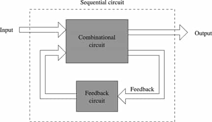
The sequential circuit is of two types.
- Synchronous Sequential Circuit: Change in input signals can affect memory elements only upon activation of clock signals.
- Asynchronous Sequential Circuit: Change in input signals can affect memory elements at any instant of time. These are faster than the synchronous circuit.
2. Flip Flops
- It is a one-bit memory cell which stores the 1-bit logical data (logic 0 or logic 1).
- It is a basic memory element.
- The most commonly used application of flip flops is in the implementation of a feedback circuit.
- As a memory relies on the feedback concept, flip flops can be used to design it.
- In the synchronous sequential circuit, Memory elements are clocked flip flops and generally edge triggered.
- In the asynchronous sequential circuit, Memory elements are unclocked flip flops/time delay elements which are generally level triggered.
- Flip flop circuit is also known as bistable multivibrator or latch because it has two stable states (1 state, 0 states).
For the electronic circuits, there are mainly four types of flip flops present.
- S-R Flip Flop (Basic Flip Flop)
- Delay Flip Flop (D Flip Flop)
- J-K Flip Flop
- T Flip Flop
Basic SR Flip Flop
- The Set-Reset (SR) flip flop is designed with the help of two NOR gates or two NAND gates.
- SR Flip Flop is also called as SR latch.
SR Latch Implementation Using NAND Gates:

Logic diagram of SR latch using NAND gates

Truth Table of Logic Diagram
SR Latch Using NOR Gates:

Logic diagram of SR latch using NOR gates

Truth Table of Logic Diagram
Clocked SR Flip Flop Implementation using NAND Gates:
It is also called a Gated S-R flip flop. The main problem with S-R flip flops is using NOR and NAND gate in the invalid state. By using a bistable SR flip-flop this problem can be overcome. This can change outputs when certain invalid states are met, regardless of the condition of either the Set or the Reset inputs.
- SR Flip Flop Using NOR Gates:

SR flip flop using NOR gates

Truth Table of SR Flip Flop
With both S=1 and R=1, the occurrence of a clock pulse causes both outputs to momentarily go to 0. When the pulse is disabled (removed), the state of the flip-flop become indeterminate, depending on whether the set or reset input of the flip-flop remains at 1 longer than the transition to 0 at the end of the pulse.
Characteristic Table

Characteristic equation of SR flip flop

Excitation Table

JK Flip Flop
A JK flip-flop eliminates the indeterminate state of the SR type. Inputs J and K is similar to the inputs S and R to set and clear the flip-flop (In JK flip-flop, the letter J is set and the letter K is for clear). When logic 1 are applied to both J and K inputs simultaneously, the flip-flop switches to its complement state. If Q=1 then it switches to Q=0 and vice versa.
- JK flip flop using SR flip flop:
S = JQ'
R = KQ

- JK flip flop using NAND latch:

- JK flip flop using NOR latch:

Characteristic Table

Excitation Table

- Characteristic equation for JK flip flop:
![]()
D-Flip Flop
D flip flop is also known as a Transparent latch, Delay flip flop or data flip flop. The D input goes directly to the S (J) input and the complement of the D input goes to the R (K) input.
- The D-flipflop has only a single data input (D).
- If D = 1, the flip-flop is switched to the set state (unless it was already set).
- If D = 0, the flip-flop switches to the clear state.

Truth Table

Characteristic Table

Excitation Table

- Characteristic equation for D-flop flop
Qn + 1 = D
T – Flip Flop
- The T flip-flop is a single input version of the JK flip-flop where T is connected to both J and K inputs directly.
- When T = 0, the flip flop enters into Hold mode, which means that the output, Q is kept the same as it was before the clock edge.
- When T = 1, the flip flop enters into Toggle mode, which means the output Q is negated after the clock edge, compared to the value before the clock edge.

Truth Table

Characteristic Table

Excitation Table

- The characteristic equation of T-Flip Flop:
Qn + 1 = T ⊕ Qn
- Race Around Condition:
- The race around condition will occur in JK flip flop when J = K = 1 and tpd (FF) < tpw.
- To avoid race around condition.
tpw < tpd (FF) < TCLK
3. Master Slave (MS) Flip Flop
- A master-slave flip-flop is constructed from two separate flip-flops. One circuit serves as a master and the other as a slave. Input clock is applied to master and Inverted clock applied to slave.

- In Master Slave, flip flop output is changed only when slave output is changing.
- The master flip-flop is enabled on the positive edge of the clock pulse and the slave flip-flop is disabled by the inverter.
- The information at the external J and K inputs is transmitted to the master flip-flop.
- When the pulse returns to 0, the master flip-flop is disabled and the slave flip-flop is enabled. The slave flip-flop then goes to the same state as the master flip-flop.
- Master is level triggered, and Slave is edge triggered
- No race around condition occurs in Master Slave flip flop.
- It stores only one bit.
4. Flip Flop Conversions
The flip flop conversions are classified into different types which are:
- SR-FF to JK-FF Conversion
- JK-FF to SR-FF Conversion
- SR-FF to D-FF Conversion
- D-FF to SR-FF Conversion
- JK-FF to T-FF Conversion
- JK-FF to D-FF Conversion
- D-FF to JK-FF Conversion
Procedure for Flip Flop conversion:
- Conversion Table: Construct the characteristic table of required flip flop (unknown), and fill available (known) flip flop excitation.
- Solve K map for given (known) flip flop as input and required flip flop as output.
- Implement the required flip flop using the known flip flop.
Example: Conversion from JK flip flop to D flip flop is shown below.


Characteristic Table

5. Registers
When a group of the flip flop is used to store a word ( a group of bits) then it is called register. To store n bits, n flip flops are cascaded in the register. If in a register, the binary information can be moved from stage to stage, this type of registers is called shift registers. According to data movement in a register, shift registers can be classified as
- Serial Input Serial Output (SISO)
- Serial Input Parallel Output (SIPO)
- Parallel Input Serial Output (PISO)
- Parallel Input Parallel Output (PIPO)
Serial Input Serial Output (SISO)

- In registers edge trigger circuit used to make circuit synchronous.
- If no clock is applied then get same data which is stored.
- In N bits SISO registers to provide N bits data, Serially in require N clock pulse, and Serially out require (N-1) clock pulse.
Serial Input Parallel Output (SIPO)

- To provide N-bit data: Serial in requires N clock pulse, and Parallel out requires no clock pulse.
- SIPO can provide n × tCIK delay to the input.
- SIPO can convert serial data or temporal code to parallel or serial code.
Parallel Input Serial Output (PISO)

- If control = 0 then it acts as parallel input;
- If control = 1 then it acts as serial output;
- To provide parallel input, one clock pulse is required.
- To provide N bits serial output, it requires (N-1) clock pulse.
- PISO can convert special code to temporal code.
Parallel Input Parallel Output (PIPO)

- In PIPO register for parallel input number of pulse required is 1 clock pulse.
- In PIPO register for parallel output number of pulse required is 0 clock pulse.
- PIPO register cannot be used as a shift register.
- It is used for temporal storage of data in microcontroller, DSP, CPU etc.
Summary of Registers

6. Counter
- A counter is a sequential logic circuit capable of counting the number of clock pulses arriving at its clock input.
- The sequence of count may be ascending, descending or non-sequence.
- For a counter circuit having n flip flops, Maximum possible states (N) = 2n
- If N = 2n , the counter acts as a binary counter.
- If N < 2n , the counter the non-binary counter.
- It counter is capable to count from 0 to 2n-1.
- MOD number is the Number of states present in a counter is known as modulus count or MOD number.
- For n-flip flops, the counter will have 2n different states then this counter is said MOD- 2n counter.
MOD-N Counter
- MOD number indicates frequency division obtained from the last flip flops.

- Cascaded two counters:

- MOD-MN counter:
- Overall states of combined counter = MN
- Input frequency = f
- Output frequency f = f/(MN)
7. Classification of Counters
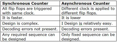
Based upon the applying clock pulse, counters are classified into two categories.
- Synchronous counter
- Asynchronous counter (ripple counter)
8. Toggle Mode Circuit
These are frequency dividers circuit.


Other Toggle Mode Circuit

9. Asynchronous Counter (Ripple counter)
- A different clock pulse is applied to different flip flops.
- All flip flops are operating in toggle mode.
- In asynchronous counter flip flop applied with external clock acts as LSB bit.
3-bit Ripple Up Counter

- Input clock is applied at LSB bit.
- It n-bit ripple counter maximum possible states are 2n.
- Bit ripple up counter counts from 0 to 2n - 1.
- If all states are used then with input frequency f, then output frequency will be f/2n
- Calculation of Time Period of Flip Flop: In n-bit ripple counter if propagation delay of each flip flop is tpd(FF), then the time period of the clock is:
![]()

- Maximum Clock Frequency:

- Due to propagation delays of flip flops decoding errors are present.
- Clear and preset are known as asynchronous input to flip flop.
- In any ripple counter, the following conditions will fulfil
- Negative edge trigger and Q as clock ⇒ up counter
- Positive edge trigger and Q as clock ⇒ up counter
3-bit Ripple Down Counter

- Positive edge trigger and Q as clock ⇒ down counter
- Negative edge trigger and Q as clock ⇒ down counter
Non-binary Ripple Counter
Decode counter or BCD counter is an example of a non-binary counter. It requires 4 flip flops.

- Used state = 10 and unused states = 6 → (24 -10)
- Output frequency of BCD counter = f/10
- For making non-binary counter clear (clr) signal is used.
- c1r is active high, and (clr)' is active low.
10. Synchronous Counters
In this type of counter, there are no connections of the first flip flop output to a clock input of the next flip flop.
Ring Counter: It is a circular shift register with only flip flop being set at any particular time, all others are cleared. It is a shift register with feedback.

- In-ring counter, if the feedback is used the number of states is reduced.
- With n flip flops maximum states = n.
- Number of unused states in-ring counter = 2n – n
- Maximum Clock Frequency: If the input frequency is f, then at the output of every flip flop we get f/N frequency. In-ring counter, if the propagation delay of each flip flop is tpd(FF) then
![]()
![]()
Johonson Ring Counter: Jhonson ring counter is also called as a Twisted ring counter, Switch tail counter, Creeping counter, or Mobies counter.

- In n - bit Jhonson counter maximum used states = 2n, unused states = 2n - 2n.
- If the input clock frequency is f, the output frequency of each flip flop is f /2n and the duty cycle is 50%.
- A disadvantage of Jhonson Ring Counter: Lockout may occur. To decode each state one, two-input AND or NOR gate is used.


Comments
write a comment