Internal Architecture of 8085 Microprocessor
The architecture of 8085 consists of three main sections, ALU (Arithmetic and Logical Unit), timing and control unit and Registers (shown in the following figure).
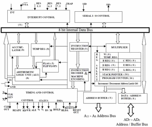
Arithmetic and Logic Unit (ALU): The ALU performs the actual numerical and logical operations.
- The ALU performs the following arithmetic and logical operations.
- Addition, Subtraction
- Logical AND, Logical OR, Logical Ex - OR
- Complement (logical NOT)
- Increment, Decrement
- Left shift, Right shift
- Clear, etc.
- ALU includes the accumulator, the temporary register, the arithmetic and logic circuits and flags. It always stores result of operations in Accumulator.
Timing & Control Unit: It generates timing and control signals, which are necessary for the execution of instructions.
- It controls data flow between CPU and peripherals (including memory).
- It provides status, control and timing signals, which are required for the operation of memory and I/O devices.
- 8085 System Bus: Microprocessor communicates with memory and other devices (input and output) using three buses: Address Bus, Data Bus and Control Bus.
- Address Bus: The Address bus consists of 16 wires. The size of the address bus determines the size of memory, which can be used. To communicate with memory the microprocessor sends an address on the address bus to the memory. Address bus is unidirectional, i.e., numbers only sent from microprocessor to memory.
- Data Bus: Bus is bidirectional. Size of the data bus determines what arithmetic can be done. Data bus also carries instructions from memory to the microprocessor.
- Memory size = 2A x D where, A denotes the address lines, and D denotes the data lines.
- Control Bus: Control bus are various lines which have specific functions for coordinating and controlling μP operations. The control bus carries control signals partly unidirectional, partly bidirectional. Control signals are things like read or write.
Registers: 8085 has six general-purpose registers to store 8 bit data, these are identified as B, C, D, E, H and L . They can be combined as register pairs BC, DE and HL to perform some 16 bit operations.
- Accumulator: The accumulator is an 8 bit register included as a part of Arithmetic Logic Unit (ALU). This register is used to store 8 bit data and to perform arithmetic and logical operations. The result of an operation is stored in the accumulator.
- Flag Register: The ALU includes five flip-flops. They are called Zero (Z), Carry (CY), Sign (S), Parity (P) and Auxiliary Carry (AC) flags. The microprocessor uses these flags to test data conditions. The conditions (set or reset) of the flags are tested through the software instructions. The combination of the flag register and the accumulator is called Program Status Word (PSW) and PSW is the 16-bit unit for stack operation.

- Program Counter (PC): This 16 bit register deals with sequencing the execution of instruction. The microprocessor uses this register to sequence the execution of the instructions. The function of the program counter is to point to the memory address from which the next byte is to be fetched.
- Stack Pointer (SP): The stack pointer is also a 16 bit register used as a memory pointer. It points to a memory location in read-write memory, called the stack.
- Instruction Register/Decoder: Temporary store for the current instructions of a program. Latest instruction sent here from memory prior to execution. Decoder then takes instruction and decodes or interprets the instruction. Decoded instruction then passed to next stage.
- Memory Address Register: Holds address, received from PC of next program instruction.
- Control Generator: It generates signal within μP to carry out the instructions which have been decoded.
- Register Selector: This block controls the use of the register stack.
- General Purpose Registers: μP requires extra registers for versatility. It can be used to store additional data during a program.
Operations of Microprocessor
The microprocessor performs the following four operations using address bus, data bus, and control bus:
- Memory Read: Reads data (or instruction) from memory.
- Memory Write: Writes data (or instruction) into memory.
- I/O Read: Accepts data from input device.
- I/O Write: Sends data to output device.
The 8085 Instruction Format
An instruction is a command to the microprocessor to perform a given task on a specified data. Each instruction has two parts, one is task to be performed, called the operation code (opcode), and the second is the data to be operated on called the operand. The 8085 instruction set is classified according to word size.
- One-Byte Instructions: A 1-byte instruction includes the opcode and operand in the same byte. Operands are internal registers and are coded into the instruction.
- Two-Byte Instructions: In a two-byte instruction, the first byte specifies the operation code and the second byte specifies the operand. Source operand is a data byte immediately following the opcode.
- Three-Byte Instructions: In a three byte instruction, the first byte specifies the opcode and the following two bytes specify the 16-bit address. Note that, the second byte is the low-order address and the third byte is the high-order address.
The 8085 Addressing Modes
The various formats for specifying operands are called the addressing modes. For 8085, they are
- Immediate Addressing:
- Data is provided in the instruction.
- Load the immediate data to the destination provided.
- Example: MVI A, 12 H
- Register Addressing:
- Data is provided through the registers.
- Example: MOV B, C
- Direct Addressing:
- Used to accept data from outside devices to store in the accumulator or send the data stored in the accumulator to the outside device.
- Example: MOV A, [1000]
- Indirect Addressing:
- Effective address is calculated by the processor and the contents of the address is used to form a second address. The second address is where the data is stored.
- Example: MOV A, [[1000]]
- Implicit addressing:
- In this addressing mode the data itself specifies the data to be operated upon.
- Example: CMA ; Complement the contents of accumulator
8085 Instruction Set
An instruction is a binary pattern designed inside a microprocessor to perform a specific function. Each instruction is represented by 8 bit binary value. Instruction set can be categorised int0 5 types:
- Data transfer instructions:
- These instructions are used to transfer data from one register to another register, from memory to register or register to memory.
- When an instruction of data transfer group is executed, data is transferred from the source to the destination without altering the contents of the source.
- Examples: MOV, MVI, LXI, LDA, STA, etc.
- Arithmetic instructions:
- These instructions are used to perform arithmetic operations such as addition, subtraction, increment or decrement of the content of a register or memory.
- Examples: ADD, ADC, ADI, DAD, SUB, INR, DCR, etc.
- Logical instructions:
- These instructions are used to perform logical operations such as AND, OR, compare, rotate etc.
- Examples: ANA, ANI, ORA, ORI, XRA, CMA, CMC , STC, CMP, RLC, RAL, RAR, etc.
- Branching Instructions:
- These instructions are used to perform conditional and unconditional jump, subroutine call and return, and restart.
- Examples: JZ, JNZ, JC, JNC, JP, JM, JPE, JPO, CALL, RET, RST, etc.
- Machine Control Instructions:
- These instructions control machine functions such as Halt, Interrupt, or do nothing.
- The microprocessor operations related to data manipulation can be summarized in four functions: copying data, performing arithmetic operations, performing logical operations, testing for a given condition and alerting the program sequence.
- Example: PUSH, POP, HLT, XTHL, NOP, EI, DI, etc.
You can avail of Online Classroom Program for all AE & JE Exams:
Online Classroom Program for AE & JE Exams (12+ Structured LIVE Courses and 160+ Mock Tests)
You can avail of BYJU'S Exam Prep Test Series specially designed for all AE & JE Exams:
BYJU'S Exam Prep Test Series AE & JE (160+ Mock Tests)
Thanks,
Team BYJU'S Exam Prep
Sahi Prep Hai to Life Set Hai !!!
Download BYJU'S Exam Prep APP , for best Exam Preparation , Free Mock Test, Live Classes


Comments
write a comment