In this article, you will find the Study Notes on Combinational Circuits-2 which will cover the topics such as Designing Combinational Circuits, Arithmetic Circuits, Mux, De-Mux, Decoders and Encoders.
1. Designing Combinational Circuits
The steps to design combinational circuits are as the following
- Understand the problem
- Find the required number of input and output variables
- Construct a truth table using the relationship between the input and output
- Obtain the Boolean function or the logical expression from the truth table using Karnaugh Map.
- Draw a logic circuit based on the obtained logical expression.
2. Arithmetic Circuits
Arithmetic circuits are used to perform addition and subtraction. Binary adder performs binary addition and binary subtractor performs binary subtraction.
Classification of Adder:
- Half Adder
- Full Adder
Classification of Subtractor:
- Half Subtractor
- Full Subtractor
Half Adder
This circuit is used for addition of two one bit numbers.
- The truth table of Half Adder:

- Half adder circuit:

Sum (S) = ![]()
Carry (C) = AB
- Implement of Half Adder Using NAND Gate:

Note: Required number of NAND Gates to implement Half Adder = 5
- Implement of Half Adder Using NOR Gate:

Note: Required number of NOR Gates to implement Half Adder = 5
Full Adder
A full adder is a combinational logic circuit that performs the arithmetic sum of three input bits. It consists of three inputs and two outputs.

- The truth table for Full Adder:
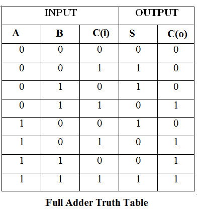
- The logic diagram of Full Adder:
Sum (S) = ![]()
Carry (C0) = AB + BC + AC

- A full adder = 2 Half adder + 1 OR Gate
- Required minimum number of NAND gate to implement FA = 9
- Required minimum number of NOR gate to implement FA = 9
Half Subtractor

- Logic Diagram of Half Subtractor:
- Difference (D)
- Borrow (B0) =
- To implement half subtractor the total number of NAND/NOR are required = 5

Full Subtractor
It is a combinational logic circuit that performs subtraction involving three bit namely minuend bit, subtrahend bit and borrows from the previous stage

- Difference (D)

- A full subtractor = 2 half subtractor + 1 OR gate
- To implement full subtractor of NAND/NOR gates are required = 9

3. Multiplexer (MUX)
- It is a combinational circuit that selects binary information from one of the many input lines and directs it to a single output line.
- The selection of a particular input line is controlled by a set of selection lines.
- MUX is also called: Many to one, Data selector, Universal circuit, or Parallel data serial.
- Multiplexing means transmitting a large number of information units over a smaller number of channels or lines. It is abbreviated as MUX.
- There are 2n input lines and n selection lines whose bit combinations determine which input is selected.
m = 2n implies n = log m where m = Number of data inputs, and n = Number of select lines.
2 × 1 MUX :

- Implementation of one MUX using another MUX:


4. Demultiplexer (DEMUX)
- It is a circuit that receives information on a single line and transmits this information on one of 2n possible output lines.
- The selection of a specific output line is controlled by the bit values of n selected lines.

1 × 2 Demux:

D0 = S′I
D1 = SI
- The truth table of 1 × 2 Demux:

1 × 4 Demux:


- The Truth table of 1 × 4 Demux:

- Circuit Diagram of 1 × 4 Demux:

- DEMUX Implementation using another DEMUX:

5. Decoders
- A decoder is a combinational circuit that converts binary information from n input lines to maximum 2n unique output lines.
- If the n-bit decoded information has unused or don’t-care combinations, the decoder output will have fewer than 2n outputs.
- The decoders presented here are n-to-m-line decoders, where m ≤ 2n. Their purpose is to generate the 2n (or fewer) minterms of n input variables.

2 × 4 Decoder:


The Truth table of 2 × 4 Decoder:

6. Encoders
- It is a combinational circuit that converts information into the coded form (binary).
- It is a digital circuit that performs the inverse operation of a decoder.
- An encoder has 2n (or fewer) input lines and n output lines.
- The output lines generate the binary code corresponding to the input value.

****


Comments
write a comment