GATE EC : Analog Circuits - National Champion Test
Attempt now to get your rank among 600 students!
Question 1
In the following circuit, V0 is
Question 2
In the bistable circuit shown, the ideal opamp has saturation level of ±5V. The value of R1 (in kΩ) that gives a hysteresis width of 500 mV is _______.
Question 3
The equivalent circuits of a diode, during forward biased and reverse biased conditions, are shown in the figure. If such a diode is used in clipper circuit of figure given above, the output voltage (v0) of the circuit will be
Question 4
The transistor amplifier with 90% of efficiency is likely to be
Question 5
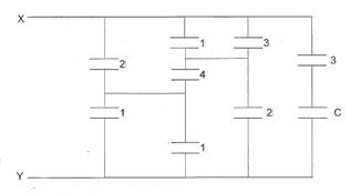
What is the value of C such that equivalent capacitance across x-y is 5µF and all capacitance are given in µF.
Question 6
Which of the following devices can be used for generating a PWM signal?
Question 7
The input impedance (Zi) and the output impedance (Z0) of an ideal transconductance (voltage controlled current source) amplifier are
Question 8
In a feedback series regulator circuit, the output voltage is regulated by controlling the
Question 9
For the circuit with ideal diodes shown in the figure, the shape of the output (υout) for the given sine wave input (υin) will be
Question 10
If each stage had gain of 10dB and noise figure of 10dB, then the overall noise figure of two-stage cascade amplifier will be
Question 11
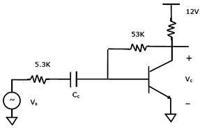
In the transistor amplifier circuit shown in the figure below, the transistor has the following parameters: βDC = 60, VBE = 0.7V, hie → ∞, hfe → ∞. The capacitance Cc can be assumed to be infinite. In the figure above, the ground has been shown by the symbol ∇.
The small-signal gain of the amplifier vc/vs is:
Question 12
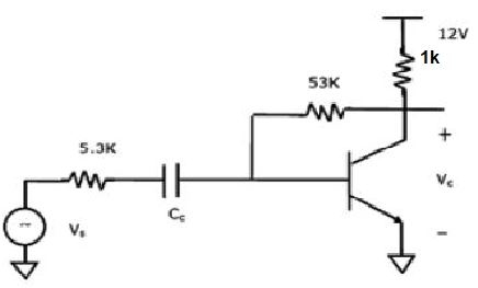
In the transistor amplifier circuit shown in the figure below, the transistor has the following parameters: βDC = 60, VBE = 0.7V, hie → ∞, hfe → ∞. The capacitance Cc can be assumed to be infinite. In the figure above, the ground has been shown by the symbol ∇.
If βDC is increased by 10%, the collector –to emitter voltage drop.
Question 13
In the transistor amplifier circuit shown in the figure below, the transistor has the following parameters: βDC = 60, VBE = 0.7V, hie → ∞, hfe → ∞. The capacitance Cc can be assumed to be infinite. In the figure above, the ground has been shown by the symbol ∇.
In the transistor amplifier circuit shown in the figure below, the transistor has the following parameters: βDC = 60, VBE = 0.7V, hie → ∞, hfe → ∞. The capacitance Cc can be assumed to be infinite. In the figure above, the ground has been shown by the symbol ∇. Under the DC conditions, the collector-to-emitter voltage drop is:
Question 14
A MOSFET in saturation has a drain current of 1 mA for VDS = 0.5 V. If the channel length modulation coefficient is 0.05 V–1, the output resistance (in kΩ) of the MOSFET is _______.
Question 15
In the CMOS inverter circuit shown, if the transconductance parameters of the NMOS and PMOS transistor are , KN=40 μA/V2and their threshold voltages are, the current I is:
Question 16
The circuit shown in the figure is used to charge the capacitor C alternately from two current sources as indicated. The switches S1 and S2 are mechanically coupled and connected as follows For 2nT ≤ t < (2n + 1) T, (n = 0,1, 2, ……) S1 to P1 and S2 to P2 For (2n + 1)T ≤ t < (2n + 2) T, (n = 0,1, 2, ……) S1 to Q1 and S2 to Q2. Assume that the capacitor has zero initial charge. Given that u(t) is a unit step function, the voltage Vc(t) across the capacitor is given be
Question 17
A voltage 1000 sin cot Volts is applied across YZ. Assuming ideal diodes, the voltage measured across WX in Volts is
Question 18
In a full-wave rectifier using two ideal diodes and center tapped transformer, Vdc and Vm are the dc and peak values of the voltage respectively across a resistive load. If PIV is the peak inverse voltage of the diode, then the appropriate relationships for this rectifier are
Question 19
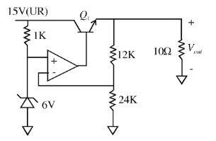
A regulated power supply, shown in figure below has an unregulated input (UR) of 15 Volts and generates a regulated output Vout. Use the component values shown in the figure. In the figure above, the ground has been shown by the symbol.
The power dissipation across the transistor Q1 shown in the figure is:
Question 20
The block diagrams of two types of half wave rectifiers are shown in the figure. The transfer characteristics of the rectifiers are also shown within the block. It is desired to make full wave rectifier using above two half-wave rectifiers. The resultant circuit will be
Question 21
Noise figure of an amplifier depends on
Question 22
For the circuit shown in the following figure, transistors M1 and M2 are identical NMOS transistors. Assume that M2 is in saturation and the output is unloaded The current Ix is related to Ibias as
Question 23
Two identical NMOS transistors M1 and M2 are connected as shown below. Vbias is chosen so that both transistors are in saturation. The equivalent gm of the pair is defined to be at constant The equivalent gm of the pair is
Question 24
In avoltage divider bias circuit what will be the equivalent Vgsq.
Question 25
The typical frequency response of a two-stage direct coupled voltage amplifier isas shown in
Question 26
The input signal Vin shown in the figure is a 1 KHz square wave voltage that alternates between +7V and -7V with a 50% duty cycle. Both transistors have the same current gain, which is large. The circuit delivers power to the load resistor RL. What is the efficiently of this circuit for the given input? Choose the closest answer.
Question 27
The approximate frequency of oscillation of the circuit shown below is
Question 28
Oscillator requires
Question 29
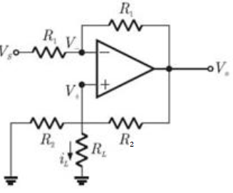
In the op-amp circuit given in Figure, the load current IL is
Question 30
What would be the output of the following circuit, if a positive going unipolar pulse with an amplitude greater than Vref, is applied at the input?