Time Left - 15:00 mins
Solution of EDC Live Session
Attempt now to get your rank among 854 students!
Question 1
A thin P-type silicon sample is uniformly illuminated with light which generates excess carriers. The recombination rate is directly proportional to
Question 2
If P is Passivation, Q is n–well implant, R is metallization and S is source/drain diffusion, then the order in which they are carried out in a standard n–well CMOS fabrication process, is
Question 3
In a Silicon Controlled Rectifier, the value of current above which it switches from the conduction state to forward blocking state is called ________.
Question 4
Consider a GaAs sample at T=300 K. Let the Hall effect device is fabricated with the following geometry: d = 0.01cm, W = 0.05 cm and L = 0.5 cm. The electrical parameters are : Ix = 2.5 mA, Vx =2.2 V and Bz = 2.5 × 10⁻² tesla. The hall voltage is VH = -4.5 mV. What will be the resistivity of the sample?
Question 5
Two GaAs wafers, one n-type and one p-type, are uniformly doped such that ND (wafer 1) = NA (wafer 2) ≥ ni , which wafer will exhibit the larger resistivity?
Question 6
If for a P-Channel JFET, we have IDSS= 30mA, VGS= 10V and VGS(off)= 20V, then determine what value of resistance 'Rs' is required in order to satisfy self-biasing method for JFET ?
Question 7
The theoretical efficiency of a class D amplifier is _______________.
Question 8
A battery of 3 volts is applied across a 1 cm long semiconductor bar. The average electron drift velocity is 104 cm/sec. Then the electron mobility is
Question 9
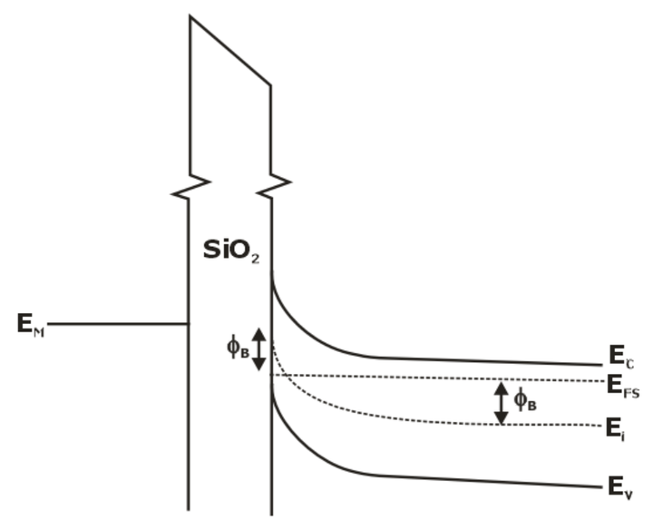
The figure shows the band diagram of a Metal Oxide Semiconductor (MOS). The surface region of this MOS is in
Question 10
The equation  (where n0 and p0 are the concentrations of the n – type and p – type carries in a given semiconductor and ni is the intrinsic carrier concentration) is valid under
- 854 attempts
- 4 upvotes
- 8 comments
Jun 7ESE & GATE EC

