Time Left - 40:00 mins
National Champion Test EE: Analog Circuits
Attempt now to get your rank among 467 students!
Question 1
In the circuit shown below what is the output voltage (Vout) in Volts if a silicon transistor Q and ideal op-amp are used?

Question 2
When a bipolar junction transistor is operating in the saturation mode, which one of the following statements is TRUE about the state of its collector-base (CB) and the base-emitter (BE) junctions?
Question 3
Which option is correct while designing a first-order active inverting low-pass filter?
Question 4
The conduction loss versus device current characteristic of a power MOSFET is best approximated by
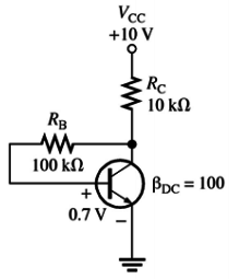
Question 5
Calculate the Q-point values (IC and VCE) for this circuit ?
Question 6
The type of power amplifier which exhibits crossover distortion in its output is
Question 7
Two diodes are connected parallel in the circuit, so what will be the current in circuit, If the diode is not ideal in the case?

Question 8
In a voltage divider bias circuit what will be the equivalent Vgsq.

Question 9
The common emitter amplifier shown in the following figure is biased using a 1 mA ideal current source. The approximate base current value is________(Given RC is 1Kohm)

Question 10
In an NMOS circuit, Vt = 4 V and VGS ranges from 7.5 to 10 V. The channel to be continuous, finds the largest value of VDS?
Question 11
In the following circuit, the transistor is in active mode and Vc = 2V. To get VC = 2V. To get VC = 4V, we replace RC with R’C. The ratio  is _____.

Question 12
A common emitter silicon transistor amplifier with quiescent emitter current as 1mA, what will be the base biasing voltage?

Question 13
What will be the value of R in the circuit, for sinusoidal oscillations of frequency of 2 kHz.

Question 14
Given that the op-amps in the figure are ideal, the output voltage V0 is

Question 15
An electronic switch S is required to block voltages of either polarity during its OFF state as shown in the following figure a. This switch is required to conduct in only onedirection during its ON state as shown in the following figure b.

Which of the following are valid realizations of the switch S?
(P)
(Q)
(R)
(S)
Which of the following are valid realizations of the switch S?
(P)
(Q)
(R)
(S)
Question 16
An amplifier without feedback has a gain of 150, input resistance of 2kΩ and output resistance of 5kΩ. The input resistance of current shunt negative feedback amplifier using the above amplifier with a feedback factor of 02 is.
- 467 attempts
- 7 upvotes
- 8 comments
Sep 16ESE & GATE EE

