Time Left - 15:00 mins
GATE 2025 EDC Quiz 18
Attempt now to get your rank among 40 students!
Question 1
The transition Capacitance of a step graded Si p-n junction diode is 20PF at a reverse bias voltage of 5V , and  if reverse bias voltage is increased by 1 v , then the change in capacitance is ______(pF)
Question 2
A metal-semiconductor junction is taken. The variation of the electric field inside the semiconductor is shown in the figure below 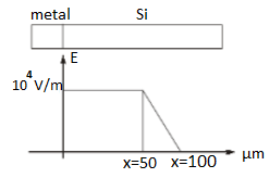
The built-in potential of the diode is _____V.
Question 3
For an npn BJT transistor, how does the common-emitter current gain β depend on the relative dopings of the base region and the emitter region, NA/ND and the width of base W?
Question 4
For the below BJT which of the following is true, for amplification process where BVCB = Breakdown voltage in CB configuration

Question 5
Consider an abrupt PN junction (at T = 300 K) shown in the figure. The depletion region width Xn on the N-side of the junction is 0.2 μm and the permittivity of silicon (εsi) is 1.044x10⁻¹² F/cm At the junction, the approximate magnitude value of the peak electric field (in kV/cm) is _________.

- 40 attempts
- 0 upvotes
- 0 comments
Nov 29ESE & GATE EC

