Time Left - 15:00 mins
GATE 2024 EDC Rank Booster Quiz 17
Attempt now to get your rank among 29 students!
Question 1
A metal-semiconductor junction is taken. The variation of the electric field inside the semiconductor is shown in the figure below 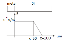
The built-in potential of the diode is _____V.
Question 2
Consider silicon diode at
 . The slope of the diffusion capacitance versus forward bias current is
 . The hole lifetime is _______
 .
.
(Assume forward bias current )
)
(Assume forward bias current
Question 3
The built-in potential for a silicon p-n junction diode with ND= 1014 cm-3 and NA= 1017 cm-3 for T=300K will be ___V?
(Given intrinsic carrier concentration ni=1.5 1010 cm3).
(Given intrinsic carrier concentration ni=1.5
Question 4
Consider an abrupt PN junction (at T = 300 K) shown in the figure. The depletion region width Xn on the N-side of the junction is 0.2 μm and the permittivity of silicon (εsi) is 1.044x10⁻¹² F/cm At the junction, the approximate magnitude value of the peak electric field (in kV/cm) is _________.

Question 5
Consider an ideal silicon P-N junction diode with the following parameters

The ratio of so that 95% of current in depletion region is carried by electron is
The ratio of
Question 6
The transition Capacitance of a step graded Si p-n junction diode is 20PF at a reverse bias voltage of 5V , and  if reverse bias voltage is increased by 1 v , then the change in capacitance is ______(pF)
Question 7
The built in potential of PN junction diode depends on
- 29 attempts
- 0 upvotes
- 0 comments
Nov 28ESE & GATE EC

