Time Left - 24:00 mins
BARC EE 2019: Analog Electronics Nuclear Mini Mock
Attempt now to get your rank among 383 students!
Question 1
In the circuit shown, the PNP transistor has  and
and  Assume that
  For
For  to be 5 V, the value of
  is ___________ .

Question 2
The desirable characteristics of a transconductance amplifier are
Question 3
For the given input waveform, a clamper produces the given output. Determine the clamper circuit.

Question 4
For the given network, determine the output waveform. The circuit components are given below:


Question 5
An input voltage as shown is applied to the given circuit, which produces a half-wave rectified output.
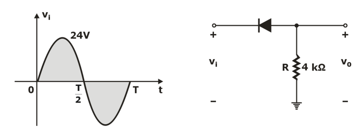
Determine the percentage drop in the dc level, if the ideal diode is replaced by a silicon diode.
Determine the percentage drop in the dc level, if the ideal diode is replaced by a silicon diode.
Question 6
A 100 pF capacitor has a maximum charging current of 150 μA. What is the slew rate?
Question 7
For the circuit shown below, assume that the OPAMP is ideal.

Which one of the following is TRUE?
Which one of the following is TRUE?
Question 8
The transistor in the given circuit should always be in the active region.Take VcE(sat)=0.2V, VEE= 0.7 V The maximum value of Rc in Ω which can be used is __________.

Question 9
In the circuit shown , function of diode D1 is

Question 10
For the given circuit, if resistance  is increased by 4 times, what is its effect on the drain current?

Question 11
The circuit shown in figure is

Question 12
Two perfectly matched silicon transistors are connected as shown in figure. The value of
the current I is

the current I is
Question 13
For the op-amp circuit shown in below, determine the output voltage υ0. Assume that the op-amps are ideal.

Question 14
In the circuit shown, the silicon BJT has ![]() Assume
Assume ![]() and
and ![]() Which one of the following statements is correct?
Which one of the following statements is correct? 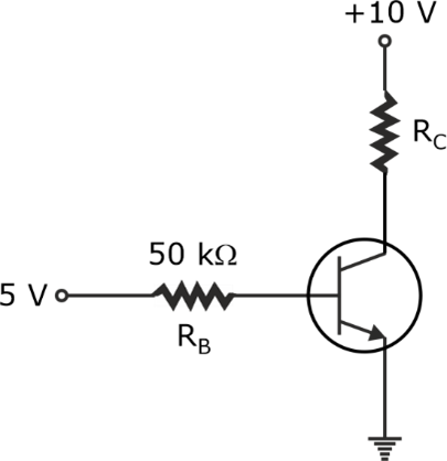
Question 15
In the circuit shown below, the range of  that will result in
  being maintained at 10 V is

Question 16
In the circuit shown in figure (a), if the input is given as in figure (b). then the output will be (Assume that the time constant is very large)


Question 17
In the circuit shown below, the current I through the transistor Q2 is _______ mA.

Question 18
Determine the output voltage for the network shown below.

Question 19
While biasing JFET if drain and source are interchanged, then
Question 20
For the circuit shown below, taking the opamp as ideal, the output voltage  in terms of the input voltages V1 ,V2 and V3 is

- 383 attempts
- 2 upvotes
- 1 comment
Jul 5ESE & GATE EE

