- Home/
- GATE ELECTRONICS/
- GATE EC/
- Article
Types of Modulation & Demodulation Study Notes for Instrumentation Engineering
By BYJU'S Exam Prep
Updated on: September 25th, 2023

Modulation and demodulation are fundamental concepts in the field of instrumentation engineering, which involve the process of modifying a carrier signal to carry information and then extracting that information from the modified signal. These concepts are widely used in various applications, including telecommunications, radio broadcasting, wireless systems, and data transmission.
In this article, you will find the Study Notes on Types of Modulation and Demodulation which will cover the topics such as Introduction to communication systems, Amplitude and Demodulation, Classification of AM, Angle modulation and Demodulation, Generation of FM and Pulse Modulation.
Table of content
-
1.
Introduction to Communication Systems

-
2.
Amplitude Modulation and Demodulation
-
3.
The concept of Negative Frequency
-
4.
Power Relation in AM Wave
-
5.
Current Relations in AM Wave
-
6.
Voltage Relations in AM Wave
-
7.
Generation of AM
-
8.
Classification of AM
-
9.
Conventional AM Over DSBSC and SB Signals
-
10.
Angle Modulation and Demodulation
-
11.
Generation of FM
-
12.
Pulse Modulation
-
13.
PCM System Block Diagram
Introduction to Communication Systems
Communication is a process by which information is exchanged between individuals through a common system of symbols. It can be explained in following ways:
- It is a technique for expressing ideas effectively
- It is a system of routes for moving troops, supplies, and vehicles
- Communication is the transfer of information from one point in space and time to another point.
Block diagram of a communication system

- Transmitter: couples the message onto the channel using high-frequency signals
- Receiver: restores the signal to its original form
- Channel: the medium used for the transmission of signals
- Modulation: the process of shifting the frequency spectrum of a message signal to a frequency range in which more efficient transmission can be achieved
- Demodulation: the process of shifting the frequency spectrum back to the original baseband frequency range and reconstructing the original form, if necessary
Amplitude Modulation and Demodulation
Modulation
- Modulation may be defined as the process by which some characteristics of a signal called carrier are varied in accordance with the instantaneous value of another signal called modulating the signal.
- The carrier frequency is greater than the modulating frequency. The signal resulting from the process of modulation is called modulating the signal.
- Types of Modulation: When the carrier wave is continuous in nature, the modulation process is known as Continuous Wave (CW) modulation or analog modulation.
- Amplitude Modulation
- Angle Modulation
Amplitude Modulation
- A system of modulation in which the envelope of the transmitted wave contains a component similar to the waveform of the signal to be transmitted.
- The envelope of the modulated carrier has the same shape as the message waveform, achieved by adding the translated message that is appropriately proportional to the unmodulated carrier.
- Amplitude modulation may be defined as a system in which the maximum amplitude of the carrier wave is made proportional to the instantaneous value (amplitude) of the modulating or baseband signal.
- Let c(t) = Vc cos ωct, and m(t) = Vm sin ωmt. Then the amplitude-modulated signal is

![]()
where η is known as the modulation index.

Frequency Spectrum of AM
- Significant frequencies from fc to (fc + fm) are called as an upper sideband.
- Significant frequencies from (fc + fm) to fc are called a lower sideband.

fc = Carrier signal frequency, and fm = Modulating signal frequency

- A signal can be transmitted in different frequency bands.
- If the signal is transmitted over its original frequency band, the transmission is called baseband transmission.
- If the signal is shifted to a frequency band higher than its original baseband, it is called passband transmission.
The concept of Negative Frequency
The negative frequency that appeared in the spectrum is due to the exponential representation of the Fourier transform. It is sufficient to consider only the positive frequency region while treating the negative frequency region as a replica of the positive frequencies. The bandwidth of AM signal can be
- Carrier signal [i.e., c(t) = Vccos 2πfct] is a fixed frequency signal having frequency ωc.
- The modulating or baseband signal x(t) contains the information or intelligence to be transmitted.
- In the process of amplitude modulation, the frequency and phase of the carrier remain constant whereas the maximum amplitude varies according to the instantaneous value of the information signal.
- The AM wave has a time-varying amplitude called the envelope of the AM wave.
- We generally keep fc ≥ fm, which ensures that the two sidebands do not overlap each other.
Modulation Index
- In AM system, the modulation index is defined as the measure of the extent of amplitude variation about an unmodulated maximum carrier.


- Vmax is the Maximum value of amplitude modulated wave, and Vmin is the Minimum value of amplitude modulated wave.
- The baseband or modulating signal will be preserved in the envelope of the AM signal only if we have
![]()
- The modulation index is less than or equal to unity.
- If μ > 1or the percentage modulation is greater than 100, the baseband signal is not preserved in the envelope.
- Minimum value of amplitude modulated wave is Vmin = (Vc – Vm)
- Maximum value of amplitude modulated wave is Vmax = (Vc + Vm)
- For avoiding phase reversal | μ | < 1
Power Relation in AM Wave
The total power PAM of the AM wave is the sum of the carrier power Pc and sideband power Ps.
![]()


![]()
- where, PLSB = Lower sideband power, PUSB = Upper sideband power, and Pc = Carrier signal power
![]()

- The maximum power dissipated in the AM wave is PAM = 1.5 Pc for μ = 1 and this is the maximum power that the amplifier can handle without distortion.
Current Relations in AM Wave
- The total power and carrier power can be represented by the following equations:

- IC is the unmodulated carrier current and IT is the total, or modulated, current of an AM transmitter.
- These currents are usually applied or measured at the antenna. Hence, R is the antenna resistance.
Voltage Relations in AM Wave
The total modulating voltage in AM wave ‘Ir in terms of carrier voltage can be given as


- where, Vt = Total modulating voltage, and Vc = Carrier voltage
Modulated by Several Sine Waves:
- Let V1, V2, V3…… etc be the simultaneous modulation voltages. Then the total modulating voltage Vt will be
![]()

![]()
- where μt is the overall modulation index, μ1, μ2, μ3 are the respective modulation index for individual waves.
![]()
- where PSB is total sideband power.

- In AM waves, transmission efficiency may be defined as the percentage of total power contributed by the sidebands.
- Transmission efficiency,
![]()


- The maximum transmission efficiency of the AM is only 33.33%. This implies that only one-third of the total power is carried by the sidebands and the rest two-third is wasted.
- In AM, it is generally more convenient to measure the AM transmitter current than the power.
- The modulation index may be calculated from the values of unmodulated and modulated currents in the AM transmitter.
Generation of AM
- The device which is used to generate an amplitude-modulated (AM) wave is known as an amplitude modulator.
- The methods of AM generation may be broadly classified as follows
- Low-level AM modulation
- High-level AM modulation
Square Law Modulator:
- Square law diode modulation and switching modulation are examples of low-level modulation because it is suited at low voltage levels (i.e., because of nonlinear V-I characteristics of the diode)

- The nonlinear relationship between voltage and current for a diode is
![]()
- Modulation index (μ or ma)
![]()
- The process of extracting a modulating or baseband signal from the modulated signal is called demodulation or detection.
- For amplitude modulation, detectors or demodulators are categorized as
- Square law detectors
- Envelope detectors
Square Law Detector
- A low-level amplitude modulated signal can only be detected by using square law detectors in which a device operating in the nonlinear region is used to detect the modulating signal.
- It usually detects a signal below 1 volt.
- The current equation is :


Envelope Detector
- AM signal with the large carrier is detected by using the envelope detector.
- The envelope detector uses the circuit which extracts the envelope of the AM wave.
- A diode operating in a linear region of its V-I characteristics can extract the envelope of an AM wave. This type of detector is known as an envelope detector or a linear detector.

- If the time constant RC is quite low, which results in large fluctuations in output voltage.
- Whereas, if the time constant RC is very large, then misses several peaks of the rectified output voltage during negative peaks.
- If RC is too low, the output voltage waveform is spiky in nature. On the other hand, if RC is too large, distortion may result due to clipping during the negative peaks of the modulation wave.
Classification of AM

- The modulated signal, which contains no carrier but two sidebands is called double sideband suppressed carrier (DSBSC) modulation.
- Let S(t) is DSBSC modulated signal, then

- The power of DSBSC Wave:


- Balanced Modulator: A balanced modulator may be defined as a circuit in which two nonlinear devices are connected in a balanced mode to produce a DSBSC signal.
- Ring Modulator: Ring Modulator is another product modulator, which is used to generate DSBSC signal. Here, we have to assume that the carrier signal c(t) is much larger than m(t) and the diode operates as on-off device.
- The DSBSC signal may be demodulated by following two methods
- Synchronous detection method
- Using envelope detector after carrier re-insertion.
- A small amount of carrier signal known as the pilot carrier is transmitted along with the modulated signal from the transmitter. This small amount of carrier signal is called a pilot carrier.
Hilbert Transform: A signal x(t) and its Hilbert transform Xh(t) has the following characteristics
- A signal x(t) and its Hilbert transform Xh(t) have the same energy density spectrum.
- A signal x(t) and its Hilbert transform Xh(t) have the same autocorrelation function.
- A signal x(t) and its Hilbert transform Xh(t) are mutually orthogonal
![]()
- If Xh(t) is a Hilbert transform of x(t), then the Hilbert transform of Xh(t) is – x(t), i.e If H[x(t)] = Xh(t), then H[Xh(t)] = – x(t)
Single Sideband Technique:
- A Single Sideband (SSB)AM signal is represented mathematically as

- where m(t) is the Hilbert transform of message signal m(t).
- (-) sign for USB and (+) sign for LSB.


- Frequency discrimination method or filter method
- Phase discrimination method or phase-shift method: The phase-shift method avoids the filter. This method makes use of two balanced modulators and two phase-shifting networks.
Conventional AM Over DSBSC and SB Signals
- The demodulation or detection of AM signals is simpler than DSBSC and SSB systems. The conventional AM can be demodulated by a rectifier or envelope detector. Detection of DSBSC and SSB is rather difficult and expensive.
- Furthermore, it is quite easier to generate conventional AM signals at high power levels as compared to DSBSC and SSB signals. For this reason, conventional AM systems are used for broadcasting purposes.
- The advantage of DSBSC and SSB systems over conventional AM systems is that the former requires lesser power to transmit the same information.
Vestigial Sideband (VSB) Modulation Technique:
- When there is a vestige or relaxation in one of the sidebands in the DSBSC signal then this is called the VSB modulation technique.
- VSB wave equation is :

- where F represents the fraction.


- Demodulation of DSBSC and SSB waves is done using a coherent carrier signal at a receiver.
- An envelope detector can also be used to recover a message by passing the received VSB signal through it.
- SSB scheme needs only one-half of the bandwidth required in the DSBSC system and less than that required in VSB also. Thus, we can say that the SSB modulation scheme is the most efficient scheme among DSBSC and VSB schemes. SSB modulation scheme is used for long-distance transmission of voice signals because it allows longer spacing between repeaters.
- A device that performs the frequency translation of a modulated signal is known as a frequency mixer. The operation often collects frequency mixing, frequency conversion, or heterodyning.
Performance Comparison of AM Techniques

Angle Modulation and Demodulation
- Angle modulation may be defined as the process in which the total phase angle of a carrier wave is varied in accordance with the instantaneous value of the modulating or message signal while keeping the amplitude of the carrier constant.
- There are two types of angle modulation schemes as under
- Phase Modulation (PM)
- Frequency Modulation (FM)
- These modulation schemes are also called nonlinear modulation schemes.
Phase Modulation (PM)
- PM is that type of angle modulation in which the phase angle φ is varied linearly with a baseband or modulating signal x(t) about an unmodulated phase angle:
![]()


- By passing the message through a differentiator, then through an FM modulator, we get a PM modulated signal.
- By passing a message through an integrator and then PM modulator we get FM modulated signal.
PM and FM Modulated Signals for Sinusoidal Message Signal:


- The amount of frequency deviation or variation depends upon the amplitude (loudness) of the modulating (audio) signal. This means that the louder the sound, the greater the frequency deviation and vice-versa.
- The frequency deviation is useful in determining the FM signal bandwidth.
- In FM broadcast, the highest audio frequency transmitted is 15 kHz.
Modulation Index: For FM, the modulation index is defined as the ratio of frequency deviation to the modulating frequency.

- The maximum modulating frequency is 15 kHz.
- The maximum frequency deviation is ± 75 kHz.
- The frequency stability of the carrier is ± 2 kHz.
- Allowable bandwidth per channel is 200 kHz.
Types of FM: The FM signal can be classified based on sensitivity constant as:
- Narrow Band FM: In this case, kf is small and hence the bandwidth of FM is narrow.
- Wide Band FM: In this case, kf is large and hence the FM signal has a wide bandwidth.
Another Representation of PM and FM Signals for Sinusoidal Message:


- By seeing the graph of the angle modulation signal we can’t tell whether it is PM or FM.
- FM receivers may be fitted with amplitude limiters to remove the amplitude variations caused by noise.
The relation between PM and FM


- It is possible to reduce noise still further by increasing the frequency deviation but in AM this is not possible.
- Standard frequency allocations provide a guard band between commercial FM stations. Due to this, there is less adjacent channel interference than in AM.
- FM broadcasts operate in the upper VHF and UHF frequency ranges at which there happens to be less noise than in the MF and HF ranges occupied by AM broadcasts.
The amplitude of the FM wave is constant. It is thus independent of the modulation depth, whereas, in AM, modulation depth governs the transmitted power.
Generation of FM
- The direct method or parameter variation method.
- The indirect method or the Armstrong method.


- Single-tuned detector circuit or balanced slope detector
- Stagger-tuned detector circuit or balanced slope detector
The following two circuits come under this category.
- Faster-Seeley detector
- Ratio detector
![]()
![]()
![]()
Superheterodyne Receiver: In a superheterodyne receiver, the incoming RF signal frequency is combined with the local oscillator signal frequency through a mixer and is converted into a signal of a lower fixed frequency.
The essential idea of the superheterodyne receiver is to change the radio frequency of the signal to a lower, fixed value, where the amplifying circuits can be designed to have great stability and gain, and proper selectivity and fidelity This lower fixed frequency is known as intermediate frequency.
Receiver Characteristics: A receiver has the following characteristics.
- Sensitivity: The sensitivity of a radio receiver may be defined as its ability to amplify weak signals.
- A superheterodyne receiver’s characteristics are discussed as under
- Selectivity: The selectivity of a receiver may be defined as the ability to reject unwanted signals. It also expresses the attenuation that the receiver offers to signal at a frequency adjacent to the one to which it is tuned.
- Fidelity: The facility is the ability of a receiver to reproduce all the modulating frequencies equally. The fidelity basically depends on the frequency response of the RF amplifier.
- Double Spotting: When a receiver picks up the same short wave station at two nearby points on the receiver dial, the double spotting phenomenon takes place. The main cause for double spotting is poor-front end selectivity i.e., inadequate image frequency rejection.
A superheterodyne receiver suffers from a major drawback known as an image frequency problem.
Pulse Modulation
Digital Transmission:
- Digital Transmission is the transmittal of digital signals between two or more points in a communications system. The signals can be binary or any other form of discrete-level digital pulses. Digital pulses can not be propagated through a wireless transmission system such as Earth’s atmosphere or free space.
- Alex H. Reeves developed the first digital transmission system in 1937 at the Paris Laboratories of AT & T for the purpose of carrying digitally encoded analog signals, such as the human voice, over metallic wire cables between telephone offices.
Advantages & Disadvantages of Digital Transmission:
- Advantages
- Noise immunity
- Multiplexing(Time domain)
- Regeneration
- Simple to evaluate and measure
- Disadvantages
- Requires more bandwidth
- Additional encoding (A/D) and decoding (D/A) circuitry
Pulse Modulation:
- Pulse modulation consists essentially of sampling analog information signals and then converting those samples into discrete pulses and transporting the pulses from a source to a destination over a physical transmission medium.
- The four predominant methods of pulse modulation:
- pulse width modulation (PWM)
- pulse position modulation (PPM)
- pulse amplitude modulation (PAM)
- pulse code modulation (PCM).
Pulse Width Modulation
- PWM is sometimes called pulse duration modulation (PDM) or pulse length modulation (PLM), as the width (an active portion of the duty cycle) of a constant amplitude pulse is varied proportionally to the amplitude of the analog signal at the time the signal is sampled.
- The maximum analog signal amplitude produces the widest pulse, and the minimum analog signal amplitude produces the narrowest pulse. Note, however, that all pulses have the same amplitude.
Pulse Position Modulation:
- With PPM, the position of a constant-width pulse within a prescribed time slot is varied according to the amplitude of the sample of the analog signal.
- The higher the amplitude of the sample, the farther to the right the pulse is positioned within the prescribed time slot. The highest amplitude sample produces a pulse to the far right and the lowest amplitude sample produces a pulse to the far left.
Pulse Amplitude Modulation:
- With PAM, the amplitude of constant width, the constant-position pulse is varied according to the amplitude of the sample of the analog signal.
- The amplitude of a pulse coincides with the amplitude of the analog signal.
- PAM waveforms resemble the original analog signal more than the waveforms for PWM or PPM.
Pulse Code Modulation:
- With PCM, the analog signal is sampled and then converted to a serial n-bit binary code for transmission.
- Each code has the same number of bits and requires the same length of time for transmission
Other Facts:
- PAM is used as an intermediate form of modulation with PSK, QAM, and PCM, although it is seldom used by itself.
- PWM and PPM are used in special-purpose communications systems mainly for the military but are seldom used for commercial digital transmission systems.
- PCM is by far the most prevalent form of pulse modulation and will be discussed in more detail.
- PCM is the preferred method of communication within the public switched telephone network because with PCM it is easy to combine digitized voice and digital data into a single, high-speed digital signal and propagate it over either metallic or optical fiber cables.
- With PCM, the pulses are of fixed length and fixed amplitude.
- PCM is a binary system where a pulse or lack of a pulse within a prescribed time slot represents either a logic 1 or a logic 0 condition.
- PWM, PPM, and PAM are digital but seldom binary, as a pulse does not represent a single binary digit ( a bit).
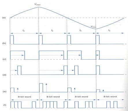
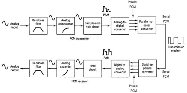
PCM System Block Diagram
- The bandpass filter limits the frequency of the analog input signal to the standard voice-band frequency range of 300 Hz to 3000 Hz.
- The sample-and-hold circuit periodically samples the analog input signal and converts those samples to a multilevel PAM signal.
- The analog-to-digital converter (ADC) converts the PAM samples to parallel PCM codes, which are converted to serial binary data in the parallel-to-serial converter and then outputted onto the transmission linear serial digital pulses.
- The transmission line repeaters are placed at prescribed distances to regenerate the digital pulses.
- In the receiver, the serial-to-parallel converter converts serial pulses received from the transmission line to parallel PCM codes.
- The digital-to-analog converter (DAC) converts the parallel PCM codes to multilevel PAM signals.
- The hold circuit is basically a low-pass filter that converts the PAM signals back to their original analog form.
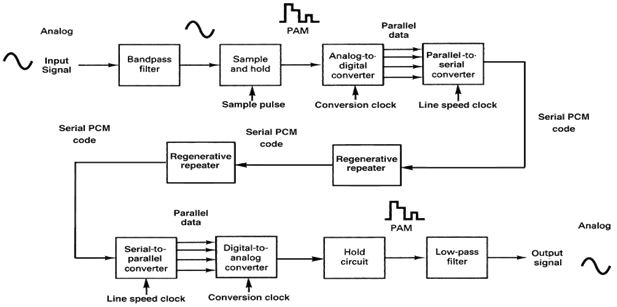
The block diagram of a single-channel, simplex (one-way only) PCM system.
PCM Sampling
- The function of a sampling circuit in a PCM transmitter is to periodically sample the continually changing analog input voltage and convert those samples to a series of constant-amplitude pulses that can more easily be converted to binary PCM code.
- A sample-and-hold circuit is a nonlinear device (mixer) with two inputs: the sampling pulse and the analog input signal.
- For the ADC to accurately convert a voltage to a binary code, the voltage must be relatively constant so that the ADC can complete the conversion before the voltage level changes. If not, the ADC would be continually attempting to follow the changes and may never stabilize on any PCM code.
- Essentially, there are two basic techniques used to perform the sampling function
- natural sampling
- flat-top sampling
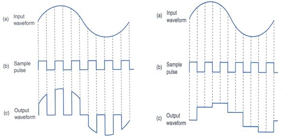 Natural Sampling on the left and Flat top sampling on right
- Natural sampling is when the tops of the sample pulses retain their natural shape during the sample interval, making it difficult for an ADC to convert the sample to a PCM code.
- The most common method used for sampling voice signals in PCM systems is flat-top sampling, which is accomplished in a sample-and-hold circuit.
- The purpose of a sample-and-hold circuit is to periodically sample the continually changing analog input voltage and convert those samples to a series of constant-amplitude PAM voltage levels.
Sampling Rate
- The Nyquist sampling theorem establishes the minimum Nyquist sampling rate (fs) that can be used for a given PCM system.
- For a sample to be reproduced accurately in a PCM receiver, each cycle of the analog input signal (fa) must be sampled at least twice.
- Consequently, the minimum sampling rate is equal to twice the highest audio input frequency.
- Mathematically, the minimum Nyquist sampling rate is:
fs ≥ 2fa
- If fs is less than two times fa an impairment called alias or foldover distortion occurs.
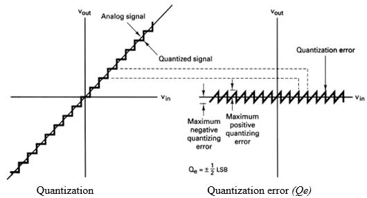
Quantization and the Folded Binary Code:
- Quantization
- Quantization is the process of converting an infinite number of possibilities to a finite number of conditions.
- Analog signals contain an infinite number of amplitude possibilities.
- Converting an analog signal to a PCM code with a limited number of combinations requires quantization.
- Folded Binary Code
- With quantization, the total voltage range is subdivided into a smaller number of sub-ranges.
- The PCM code shown in Table is a three-bit sign-magnitude code with eight possible combinations (four positive and four negative).
- The leftmost bit is the sign bit (1 = + and 0 = -), and the two rightmost bits represent magnitude.
- This type of code is called a folded binary code because the codes on the bottom half of the table are a mirror image of the codes on the top half, except for the sign bit.
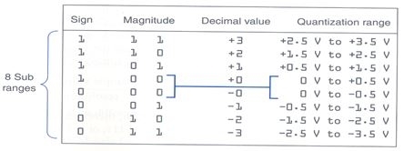
Quantization key points:
- With a folded binary code, each voltage level has one code assigned to it except zero volts, which has two codes, 100 (+0) and 000 (-0).
- The magnitude difference between adjacent steps is called the quantization interval or quantum.
- For the code shown in Table 10-2, the quantization interval is 1 V.
- If the magnitude of the sample exceeds the highest quantization interval, overload distortion (also called peak limiting) occurs.
- Assigning PCM codes to absolute magnitudes is called quantizing.
- The magnitude of a quantum is also called the resolution.
- The resolution is equal to the voltage of the minimum step size, which is equal to the voltage of the least significant bit (Vlsb) of the PCM code.
- The smaller the magnitude of a quantum, the better (smaller) the resolution and the more accurately the quantized signal will resemble the original analog sample.
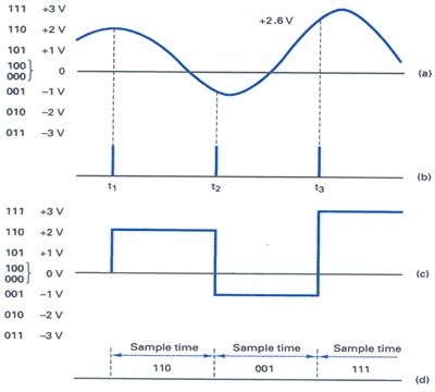
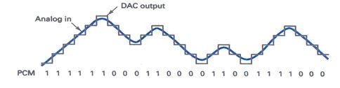
- For a sample, the voltage at t3 is approximately +2.6 V. The folded PCM code is
- sample voltage/resolution = 2.6/1 = 2.6
- There is no PCM code for +2.6; therefore, the magnitude of the sample is rounded off to the nearest valid code, which is 111, or +3 V.
- The rounding-off process results in a quantization error of 0.4 V.
- The likelihood of a sample voltage being equal to one of the eight quantization levels is remote.
- Therefore, as shown in the figure, each sample voltage is rounded off (quantized) to the closest available level and then converted to its corresponding PCM code.
- The rounded-off error is called the called the quantization error (Qe).
- To determine the PCM code for a particular sample voltage, simply divide the voltage by the resolution, convert the quotient to an n-bit binary code, and then add the sign bits.
Linear input-versus-output transfer curve:
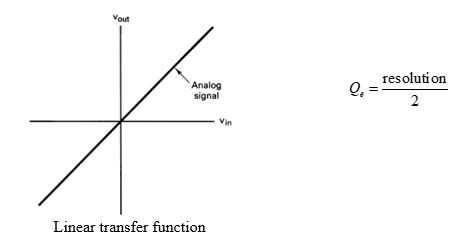
- For the PCM coding scheme shown in the figure, determine the quantized voltage, quantization error (Qe), and PCM code for the analog sample voltage of + 1.07 V.
- To determine the quantized level, simply divide the sample voltage by resolution and then round the answer off to the nearest quantization level:
- +1.07V/1V = 1.07 = 1
- The quantization error is the difference between the original sample voltage and the quantized level, or Qe = 1.07 -1 = 0.07
- From Table, the PCM code for + 1 is 101.
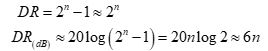
Dynamic Range (DR):
- It determines the number of PCM bits transmitted per sample.
- Dynamic range is the ratio of the largest possible magnitude to the smallest possible magnitude (other than zero) that can be decoded by the digital-to-analog converter in the receiver. Mathematically,
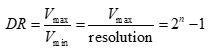
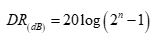
- DR= 20 log (Vmax/Vmin)
- where DR = dynamic range (unitless)
- Vmin = the quantum value
- Vmax = the maximum voltage magnitude of the DACs
- n = number of bits in a PCM code (excluding the sign bit)
- For n > 4,
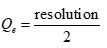
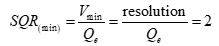
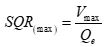
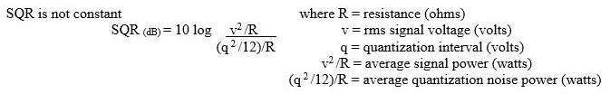
Signal-to-Quantization Noise Efficiency:
- For linear codes, the magnitude change between any two successive codes is the same.
- Also, the magnitude of their quantization error is also same.
- The maximum quantization noise is half the resolution. Therefore, the worst possible signal voltage- to-quantization noise voltage ratio (SQR) occurs when the input signal is at its minimum amplitude (101 or 001). Mathematically, the worst-case voltage SQR is
- SQR = resolution/Qe = Vlsb/ Vlsb /2
For input signal minimum amplitude:
- SQR = minimum voltage/quantization noise
For input signal maximum amplitude:
- SQR = maximum voltage/quantization noise
Linear vs. Nonlinear PCM codes:

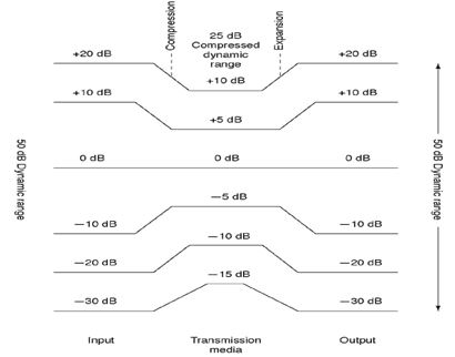
Companding:
- Companding is the process of compressing and then expanding
- High amplitude analog signals are compressed prior to txn. and then expanded in the receiver
- Higher amplitude analog signals are compressed and Dynamic range is improved
- Early PCM systems used analog companding, where as modern systems use digital companding.
 Basic companding process
Analog companding:
 PCM system with analog companding
- In the transmitter, the dynamic range of the analog signal is compressed and then converted o a linear PCM code.
- In the receiver, the PCM code is converted to a PAM signal, filtered, and then expanded back to its original dynamic range.
- There are two methods of analog companding currently being used that closely approximate a logarithmic function and are often called log-PCM codes.
- The two methods are
- μ-law
- A-law
μ-law companding:
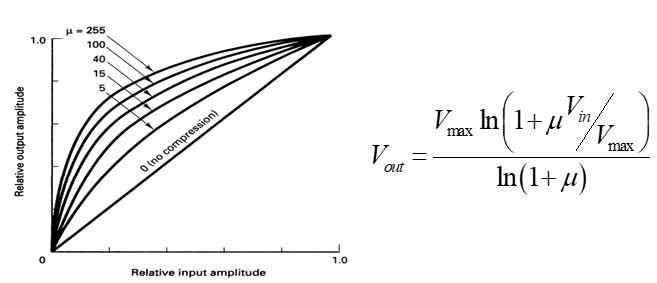
- where Vmax = maximum uncompressed analog input amplitude(volts)
- Vin = amplitude of the input signal at a particular instant of time (volts)
- μ = parameter used to define the amount of compression (unitless)
- Vout = compressed output amplitude (volts)
A-law companding:
- A-law is superior to m-law in terms of small-signal quality
- The compression characteristic is given by
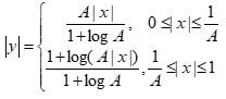
- where y = Vout
- x = Vin/Vmax
Digital Companding:
- With digital companding, the analog signal is first sampled and converted to a linear PCM code, and then the linear code is digitally compressed.
- In the receiver, the compressed PCM code is expanded and then decoded back to analog.
- The most recent digitally compressed PCM systems use a 12- bit linear PCM code and an 8-bit compressed PCM code.
Digital compression error:
- To calculate the percentage error introduced by digital compression

PCM Line speed:
- Line speed is the data rate at which serial PCM bits are clocked out of the PCM encoder onto the transmission line. Mathematically,
- Line speed= samples/second X bits/sample
Delta Modulation:
- Delta modulation uses a single-bit PCM code to achieve digital transmission of analog signals.
- With conventional PCM, each code is a binary representation of both the sign and the magnitude of a particular sample. Therefore, multiple-bit codes are required to represent the many values that the sample can be.
- With delta modulation, rather than transmit a coded representation of the sample, only a single bit is transmitted, which simply indicates whether that sample is larger or smaller than the previous sample.
- The algorithm for a delta modulation system is quite simple.
- If the current sample is smaller than the previous sample, a logic 0 is transmitted.
- If the current sample is larger than the previous sample, a logic 1 is transmitted.
Differential DM:
- With Differential Pulse Code Modulation (DPCM), the difference in the amplitude of two successive samples is transmitted rather than the actual sample. Because the range of sample differences is typically less than the range of individual samples, fewer bits are required for DPCM than for conventional PCM.
Online Classroom Program
BYJU’S Exam Prep Test Series
All the Best.
Team Byjus Exam Prep!