
AND Gate Truth Table and Circuit Diagram
By BYJU'S Exam Prep
Updated on: September 25th, 2023
The AND gate is one of the digital system’s primary or fundamental logic gates. A logic gate is a physical device that performs a logical operation in one or more logical fain-in or inputs and produces a logical output. The output of a “AND Gate” only returns “HIGH” when all the inputs are “HIGH”.
If we want to use the And gate, then the IC7408 is used in four independent gates, each of which performs the logical AND operation. Here, we will discuss AND gate in detail, along with its truth table, properties and circuit diagram.
Table of content
What is AND Gate?
The AND gate will have two or more fan-in or inputs but only one output. A logical AND gate function effectively finds the minimum between two binary digits.
AND Gate Symbol
The logic symbol two-input AND gate is:
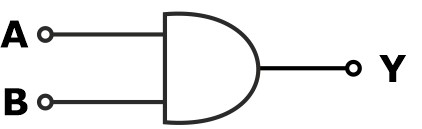
The output of the two or more fan-in or input is said to be ‘true’ or ‘1’ when all the connected fa-in or inputs is ‘true’ or ‘1’. Otherwise, the output becomes zero if any fan-in or input is ‘0’.
AND Gate Truth Table
The AND gate truth table is for the two fan-in or inputs, A and B. It has only one output as Y. The output is logic ‘0’ if any inputs A and B are LOW (logic ‘0’). However, the output is 1 only when all the inputs are 1. The AND gate truth table is as follows:
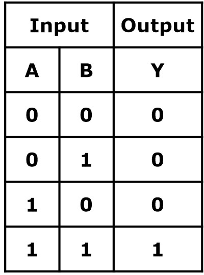
The logical expression from the above AND gate truth table is Y= AB.
Properties of AND Gate
The AND gate follows commutative property. That is, if we have two inputs, A and B, then AB = BA. Let us suppose the input A is ‘1’ and B is ‘0’, so the output Y is ‘0’ as per the given AND gate truth table. The same output we get in the commutative property as:
AB = 1.0 = 0
BA = 0.1 = 0
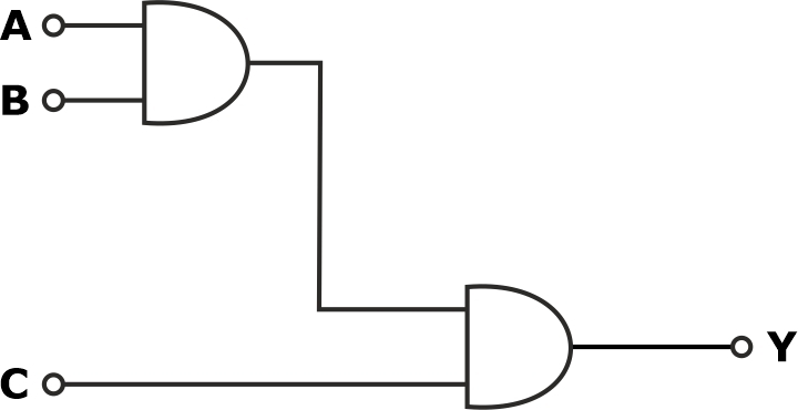
The AND gate also follows associative property. If we have three inputs, A, B and C, then (AB)C= A(BC). Let us suppose the input A is ‘1’, B is ‘0’, and C is ‘0’, so the output Y is ‘0’ as per the AND gate truth table. The same output we get in the commutative property as:
(AB)C =(1.0).0 = 0.0 = 0
A(BC) =1.(0.0) = 1.0 = 0
For AND operations, we have enabled and disabled inputs that are as follows:
If control = 0; the truth table will be:
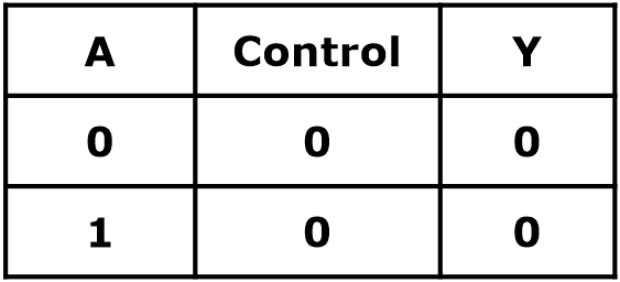
No change in the output. Hence logic ‘0’ is considered as disabled input for AND gate.
If control = 1; the truth table will be:
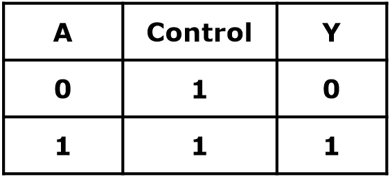
Due to change in the input-output also changes; therefore, logic ‘1’ enables input for AND gate.
Circuit Diagram of AND Gate
Based on the above AND gate truth table, the switching circuit diagram of AND gate is shown below. We have two inputs or switches, A and B, connected serially, and one blub is also connected serially with two inputs the circuit diagram of AND gate is as follows:
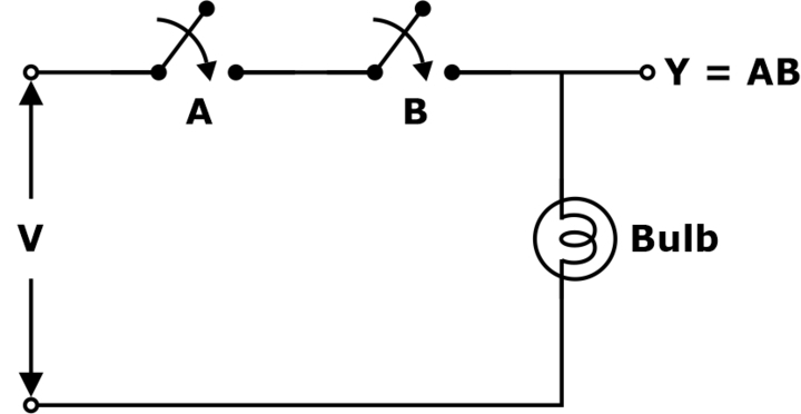
The bulb will only glow when switches A and B are closed or at logic ‘1’. If any switches A and B are open or logic ‘0’, then the bulb will not glow.


